NFC Energy-Harvesting PCB Business Card with an MCU
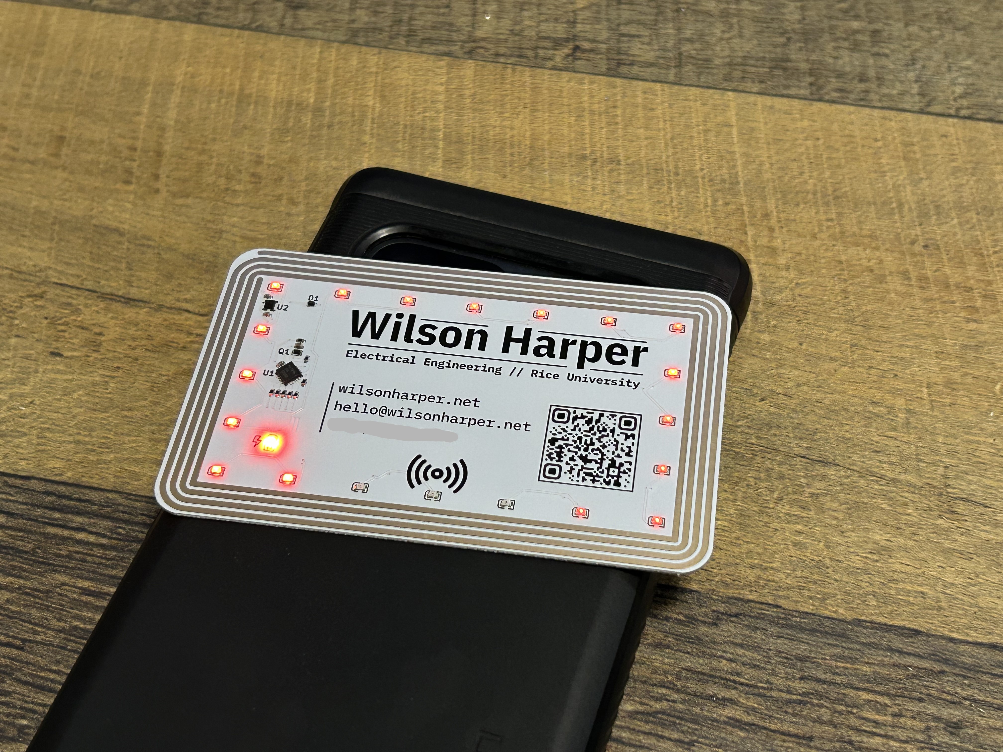
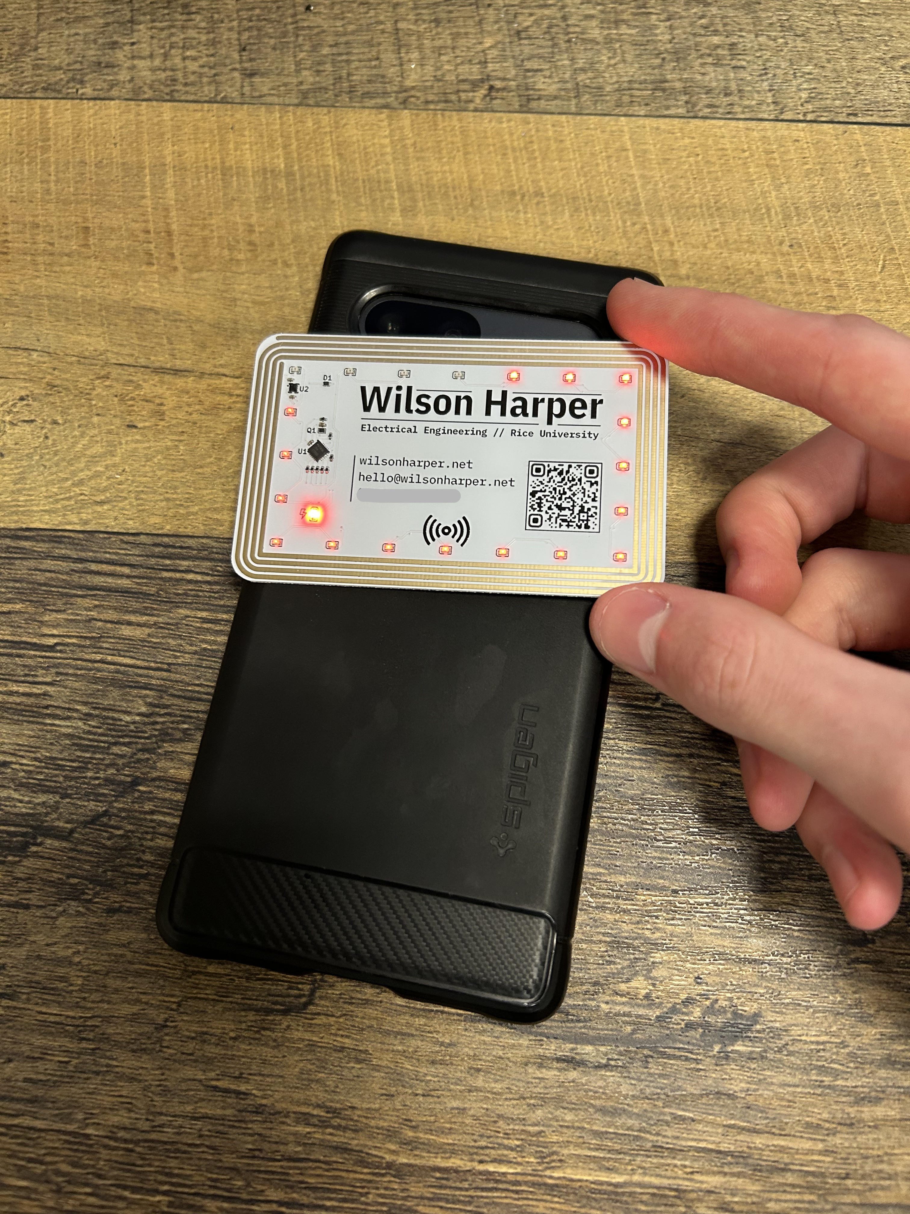
Like most business cards, mine doesn’t have a battery. When it’s tapped against a phone, though, 21 LEDs start an animation, powered just by NFC.
This project started about three months ago as an easy way to learn KiCad before jumping into more complex designs. “Easy” didn’t last long. This final product taught me more about every aspect of the PCB process than I could have expected, and the result turned out way better than I imagined. The full repo is here.
I’ve seen all sorts of business cards done on PCBs. Most that I’ve seen use the silkscreen and maybe exposed copper to include contact details and a QR code. These are really cool–but they’re more about graphic design than electrical engineering. Others include more complicated features like displays, batteries, and inputs–super cool, but expensive and thick.
I wanted to make something simple and cheap enough to be able to give to people. Eventually, I stumbled upon NFC business cards. This concept was perfect: no battery required, some basic RF engineering, and a cheap BOM. Once I started looking into specific NFC chips, I realized a few even have the ability to harvest NFC energy for other components–most notably, the NXP NTAG I2C Plus and the STMicro ST25DV-KC.
I should explain how NFC works: Your phone continuously emits a small magnetic field. An NFC card picks up on that field, making your phone act like a tiny wireless charger. The card never actually transmits a message back to your phone. Instead, it changes how much energy it absorbs from the field, and your phone detects those power dips and converts them to binary data. Most NFC tags use this harvested energy only to run their internal circuitry, but some NFC chips are able to take excess DC voltage and route it out to external hardware. This business card uses that last feature.
The theory didn’t seem too complicated. I quickly made a schematic in KiCad. The ATtiny412 microchip was an easy choice with its compact size, sufficient GPIOs, and very low power requirements.
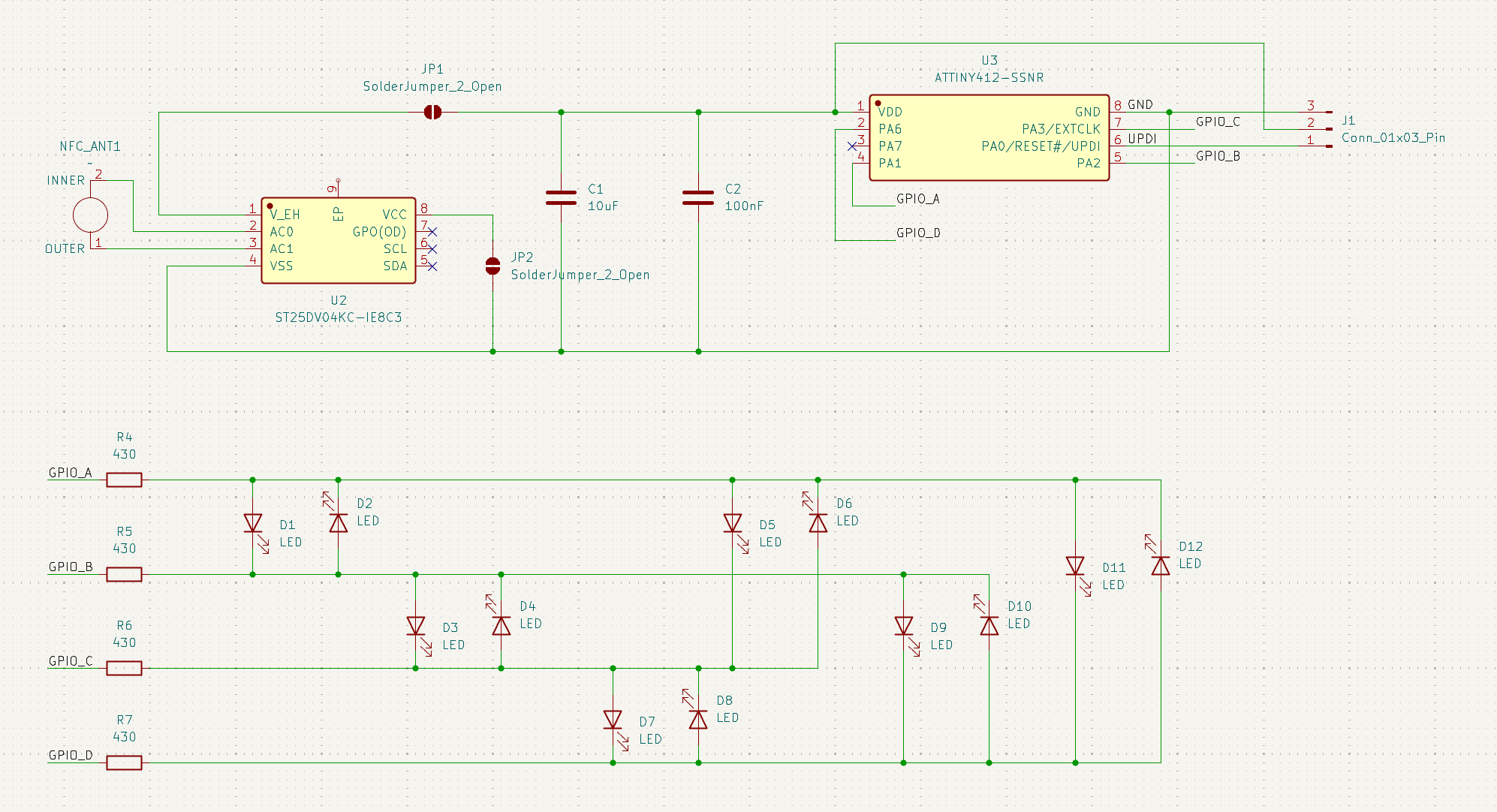
The LEDs are connected using a technique called Charlieplexing, exploiting the unidirectional current flow inherent to diodes. That Wikipedia article is a great guide to it, but the key is that tri-state logic can be used to have a few GPIOs control many LEDs. Specifically, the formula is: y = x⋅(x-1) where y represents the number of LEDs that can be independently controlled, and x represents the number of GPIOs. The primary downside is that only one LED can be lit at a time, but that can be mitigated by using PWM and spreading duty cycles across multiple LEDs. For this first draft, I used 4 GPIOs (`GPIO_A` through `GPIO_D`) to control 12 LEDs.
- * *
System Architecture
While I initially chose an ATtiny412 MCU, I realized it was suboptimal for a few reasons. It only has 5 GPIOs and comes only in through-hole/leaded-pin packages, not QFN, making it sit taller off the PCB.
Because I was away from college this summer, I didn’t have a way to assemble PCBs, so I needed to have JLCPCB assemble them for me. Also, if I planned on giving these to people, I didn’t want any lead in them, and I don’t have access to a lead-free electronics workspace even back at college. JLCPCB supports full RoHS compliance, so it was an easy choice.
Since I was getting it professionally assembled anyway, I might as well go with a much smaller QFN package, which the ATtiny412 does not come in. After some research, I found the ATtiny816. It’s similar to the ATtiny412 but with 17 GPIOs and a much thinner 3 mm × 3 mm package. Now, I could dedicate six GPIOs to LEDs, enabling me to have 20 Charlieplexed LEDs and a simple indicator LED that goes from a GPIO to `GND`. I also switched to the NXP NTAG I2C Plus NFC chip because it supports a closer-range, higher-powered NFC standard.
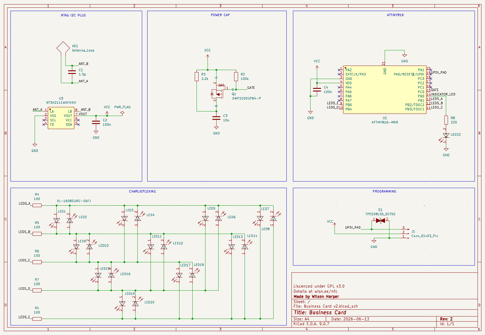
As I was reading through the NTAG I2C Plus datasheet, I noticed it specified that there shouldn’t be more than 220 nF of capacitance on `VOUT` because a larger capacitor would cause the voltage rail to drop, creating an oscillating loop that could never power on. I wanted more than 220 nF, though, so I made this circuit:
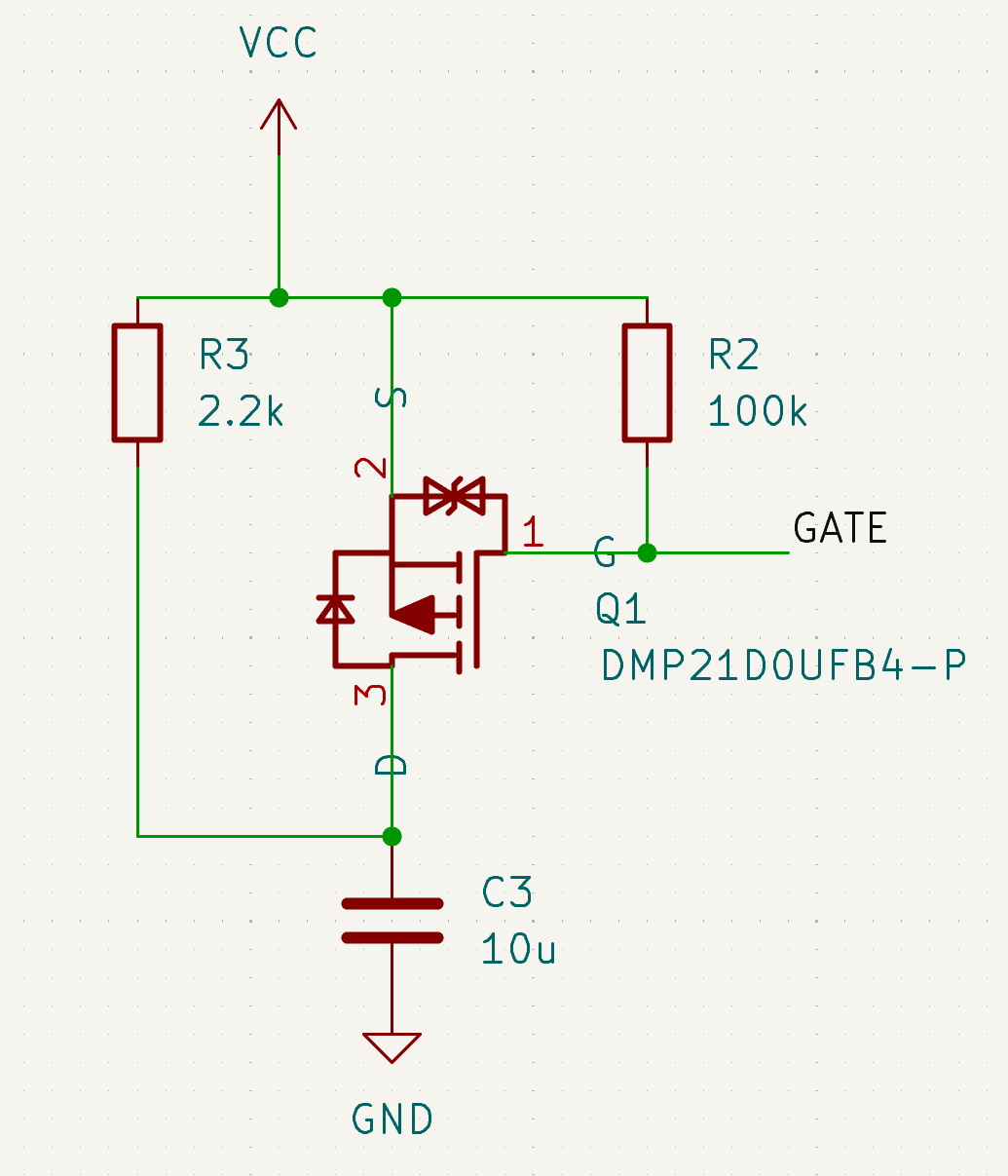
The large 10 µF capacitor at the bottom helps smooth out `VCC`, but it would draw too much current at startup. `R3` limits inrush current to just a few mA. Once the capacitor becomes charged, though, `R3` would slow the capacitor down too much. The MOSFET, `Q1`, acts as a switch. After 120 ms, `C3` is fully charged. The MCU pulls `GATE` low, giving the capacitor a low-impedance path to smooth voltage drops. `R2` is just a pull-up resistor to keep `GATE` high for the first 120 ms. This creates a circuit with the benefits of a large capacitor without ignoring the datasheet.
I decided to use 100 Ω resistors on each of the Charlieplexed traces. The total resistance is effectively doubled because current must flow out of one GPIO, through the resistor, through the LED, and then through another resistor. I also realized that if 100 Ω resistors allowed too much current, I could PWM the LEDs at a high frequency. With the 10 µF capacitor, these pulses would smooth to a steady current, preventing `VOUT` from collapsing. At a 1 kHz refresh and 20% duty cycle, the math indicates that `VOUT` drops by about 0.2 V.
- * *
Making the Antenna
I determined the dimensions and properties of the antenna using STM’s antenna inductance tool. I wanted the antenna to take up the full space of the card, so I just played around with turn count, trace width, and trace spacing until I found a combination that worked well. I needed the inductance to be close to 2.75 µH so it would resonate at 13.56 MHz with the NTAG’s internal 50 pF capacitor. This worked:
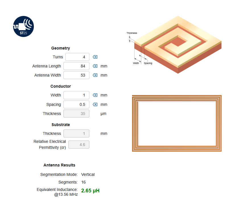
Because this inductance is a bit lower, it gives me the ability to tune it to exactly the right frequency. If it were already exactly 2.75 µH, I could add a capacitor in parallel to decrease the resonant frequency–but there’d be no way to increase it. I populated a 1.5 pF capacitor so I could tune it lower if needed.
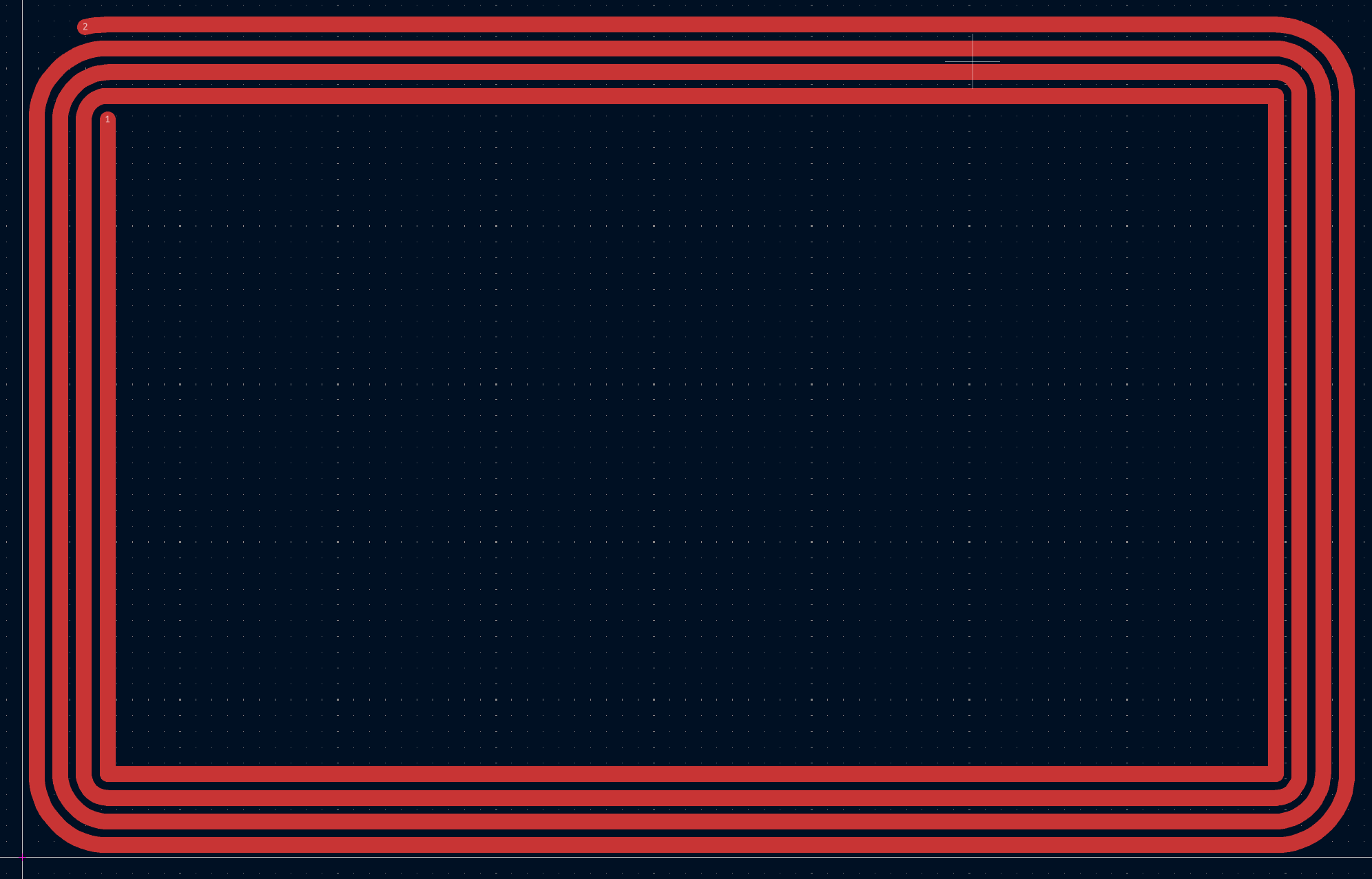
I went ahead and routed the PCB. I was surprised that KiCad doesn’t offer a built-in antenna or coil generation tool, and all the plug-ins I tried were not capable of a rectangular spiral. A KiPython script was the answer. An LLM helped create the script, and it was working after a few minutes of conversation. It generates a simple rectangular-spiral trace that matched the numbers I put into the SMT calculator. I’ve included the `.py` file in the repo, and I could see it being genuinely useful for others. Afterward, I rounded the corners by hand–this modification changed the enclosed area by just a few percent.
- * *
Layout
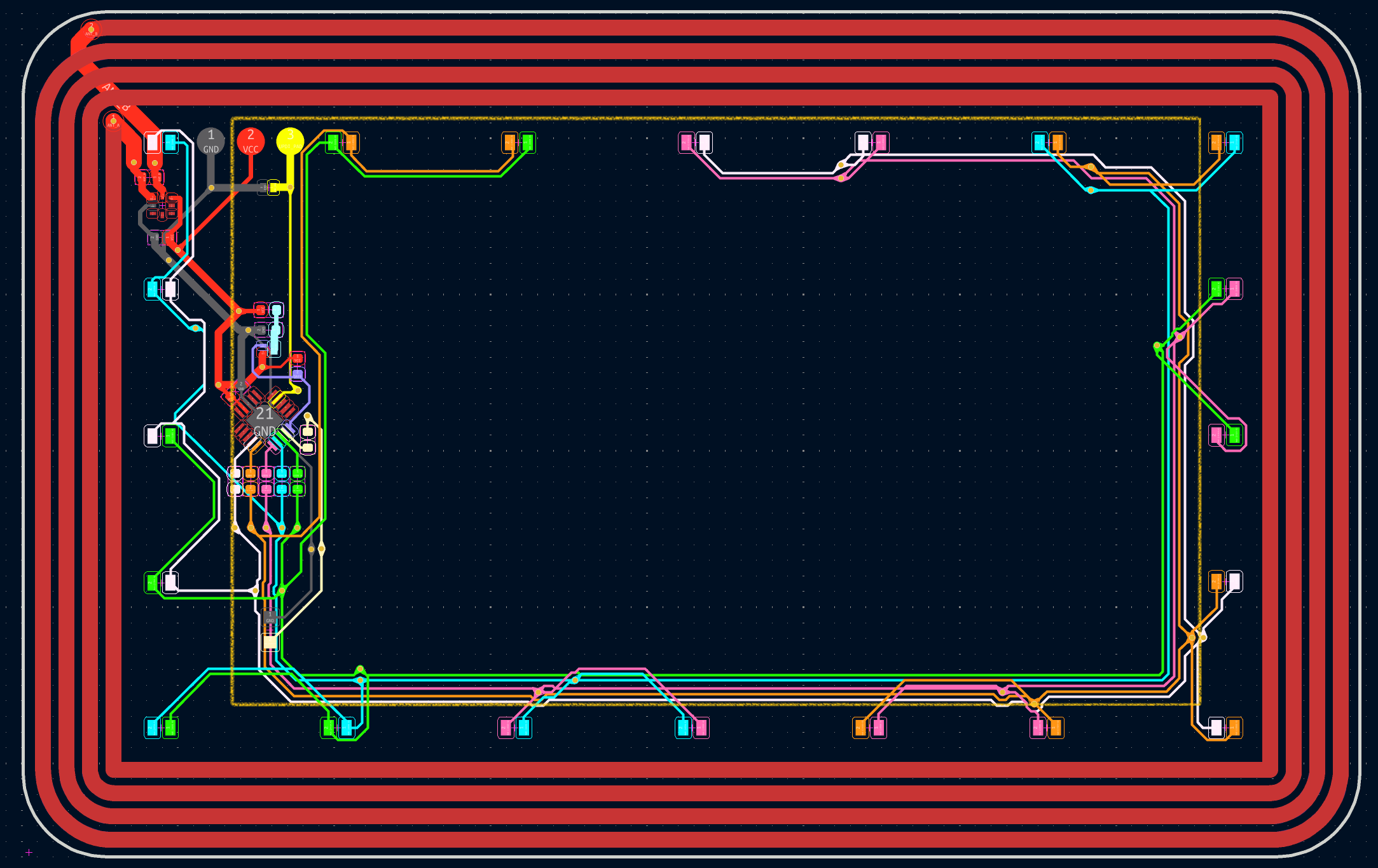
I thought it’d be aesthetically pleasing to keep all ICs and passive components to the left quarter of the PCB. I routed, deleted, and rerouted the traces for the LEDs something like six times, and I settled on this design. While it is possible to route the traces in a way that results in a shorter average trace length, I wanted to avoid creating a full loop–and I also wanted to minimize loop area. With a full loop, the traces would couple with the NFC field and create destructive eddy currents. By leaving the gap in the top middle of the loop, no currents are able to form, so the antenna remains unaffected by macro-scale RF interference.
Net colors made it easier (and more fun) to understand which trace goes where. The ribbon topology does still create enclosed current between each trace, a separate effect from the main loop. Keeping trace spacing and width minimal helped.
- * *
Back Design
I decided to show all traces on the back of the card. I also created a simple block diagram and IC BOM. To copy the traces to the `B.Silkscreen` layer, I plotted `F.Cu` and `B.Cu` as `.SVGs` and imported them onto `B.Silkscreen`, aligning them by eye. The routing is unusual in many ways, and I am sure a seasoned electrical engineer would notice changes worth making. I’m sure more than one person is reading this and thinking _Why didn’t he use a ground plane?_ A ground plane would prevent all flux through the antenna, killing it.
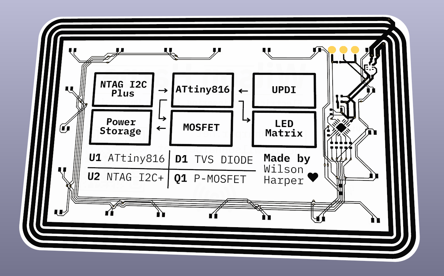
With my goals of minimizing enclosed current and creating an interesting and pleasing aesthetic, I think the end result is solid.
- * *
Fabrication and Assembly
The cards are the same dimensions as a credit card, and I paid a bit extra to make them just as thin. I also opted for high-precision silkscreen printing and an ENIG finish. With that last choice, the cards are fully RoHS-compliant–no lead or other hazardous substances.
When I went to purchase, I had to make a decision: Should I order just a few to see if they work, or should I commit all the way? After hours in JLCPCB’s quoting tool, I realized the marginal cost of each additional card was tiny, and the difference between purchasing five and thirty wasn’t huge. I bit the bullet, crossed my fingers, and ordered thirty.
When it first arrived, I started by testing if it could even harvest power. I hooked up an LED across `VCC` and `GND`, and it worked, no tuning needed.
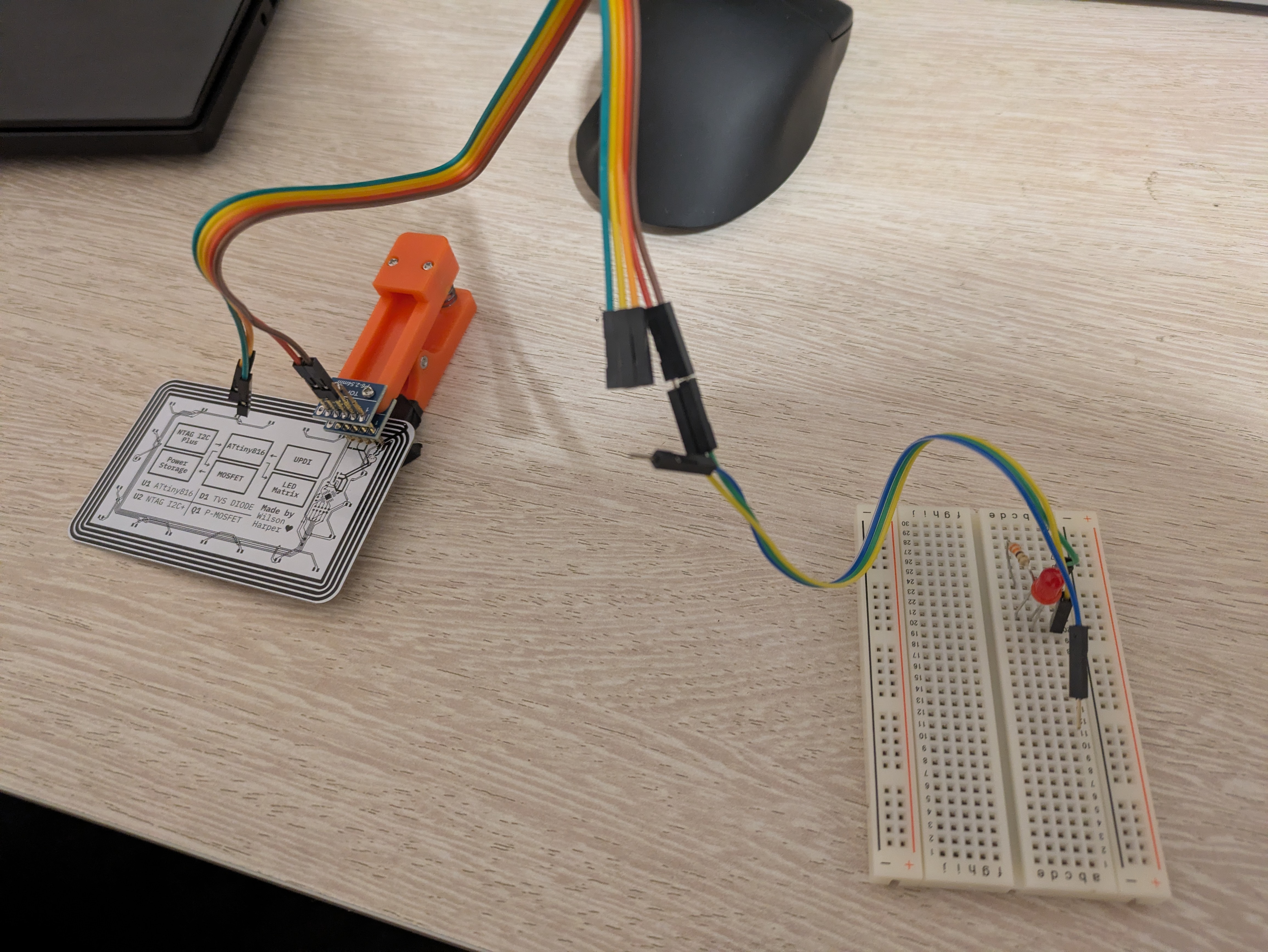
Of course, it’s hard to take a picture of the card while it’s against the back of the phone.
- * *
Programming
I have three small exposed pads on the back: `GND`, `VCC`, and `UPDI`. This order of pads–similar to RC servos–prevents any damage if the connection is rotated 180 degrees. Each pad is 1.8mm in diameter with a center-to-center distance of 0.1”/0.254mm. This standard breadboard distance allows me to use a Pogo Pin Clip to connect to it without adding another component. Business cards are handled roughly and thrown in static-y wallets and pockets, so I added a TVS diode bridging `UPDI` and `GND` so any high voltage flows straight into ground instead of frying the MCU.
The ATtiny816 is programmed over UPDI–Unified Program and Debug Interface. It’s basically UART but in a single-wire format. There are official debuggers, and USB-to-serial adapters can work too. People have also used Arduinos and RPi Picos as programmers, and that last option sounded like the most fun. The majority of Arduinos that support the jtag2updi firmware have 5V logic levels, so I had to go with a Pico. I found a `UF2` file, wired everything up, and… nothing happened. I spent hours working through IDE settings and trying different pins. Finally, I had the bright idea to hook up its output to an oscilloscope. Nothing happened. I felt very silly and decided to order the Adafruit UPDI Friend. It worked instantly.
The code itself is similar in some ways to a basic blinking Arduino sketch. However, I wrote the main loop in bare-metal C so the Charlieplexed matrix could loop as fast as possible, keeping flicker to a minimum. There’s also an easter egg in the code–see if you can find it. I downclocked the ATtiny to 1 MHz, saving power.
The NTAG I2C Plus is ironically not connected to the ATtiny through I2C. To program it, I initially used the well-known NFC Tools Android app. After some errors, I realized the NXP TagWriter app worked much better to format and write my contact info to the card.
The QR code and NFC link both direct devices to https://connect.wilsonharper.net. Currently, that just redirects to https://wilsonharper.net, but I can configure it in Cloudflare to route to any URL without any hardware changes.
- * *
Bill of Materials
View full BOM details here.
- * *
Lessons Learned
The thirty cards I have now should last a while. Once I do run out, though, I plan to make a V2. `VOUT` stays at a high enough voltage to power any color of LED, and green or yellow could be interesting. I’m also considering adding a thin button or two for interactivity, and there are several arcade-style games I could make with a ring of LEDs.
“Hardware is hard” is a phrase I’ve heard frequently, and this project made me realize how true it is. Individually, nothing in this project is novel or even that complicated: NFC PCB antennas, blinky LEDs with an MCU, and PCB business cards have all been done before. As far as I can tell, though, no one has combined them into one aesthetically-pleasing package–or, at least, I couldn’t find an example anywhere online (there are several that have NFC harvesting, circuitry in the antenna, or Charlieplexing, but not all three). There were moments where I felt sure this was beyond my capabilities. After triple-checking every possible issue, I realized I just had to send it, and I’m so glad I did.