Micron: HBM Requires Three Times More Wafer Area Than DDR5
📖 Reading time: approx. 5 minutes · 996 words · 6,341 characters
HBM has become roughly as optional for modern AI accelerators as memory itself. However, its extremely high bandwidth comes at a manufacturing cost that goes far beyond elaborate packaging. At Hot Chips 2026, Micron drew a notable comparison: For the same memory capacity, HBM requires approximately three times the wafer area of DDR5. And anyone hoping that upcoming generations would make this ratio more favorable again is likely to receive bad news from Micron. The statement comes from the presentation “Evolving memory architectures for AI” by Raghu Sreeramaneni, HBM Design Architecture Fellow at Micron, which took place on August 23, 2026, as part of Hot Chips. The event and Micron presentation are confirmed by the official program.

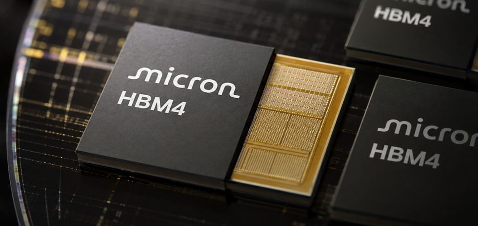
Symbolic image / generated concept image
The specific statements regarding the threefold wafer area come from current reporting on the presentation and therefore should not be equated with a separate Micron press release. A technical detail is important here. According to Sreeramaneni’s statements, the factor of three is based on a comparison of HBM3E with DDR5 and is already a somewhat older estimate according to him. When asked whether this ratio would improve with newer generations, the Micron Fellow reportedly explained that it definitely would not get better. HBM achieves its bandwidth through considerably greater parallelism. According to the data shown at Hot Chips, an HBM4 die, for example, operates with 256 memory banks, while DDR5 is specified with 32. Additional data paths, the power supply, and the Through-Silicon Vias, which connect the stacked memory dies to one another, must also be taken into account.
| Feature | HBM | DDR5 | | --- | --- | --- | | Wafer area at the same capacity | approximately a factor of 3 in the HBM3E comparison | Reference value | | Memory banks in the comparison shown | up to 256 with HBM4 | 32 | | Structure | stacked DRAM dies with TSVs | conventional DRAM organization | | Optimization target | maximum parallel bandwidth | capacity, cost, and general system memory | | Manufacturing effort | very high | considerably lower |
This is decisive because more wafer area per stored bit also means that a given HBM capacity consumes a larger share of the available DRAM manufacturing capacity. The reason manufacturers nevertheless accept this effort can be seen in Micron’s current HBM4. The interface has been widened to 2,048 I/Os. Micron specifies pin speeds of more than 11 Gbit/s and memory bandwidth of over 2.8 TB/s per stack. According to the manufacturer, this corresponds to a 2.3-fold increase in bandwidth compared with Micron’s HBM3E. At the same time, energy efficiency is expected to improve by more than 20 percent.
However, these figures do not come at no cost. Greater parallelism, higher pin speeds, increasing stack heights, and larger dies increase the requirements for silicon area and packaging. According to the report on Sreeramaneni’s presentation, the relative area requirement will therefore tend to increase further with upcoming HBM generations. This makes it easier to understand why the HBM boom can have such a major impact on the entire DRAM industry. A memory manufacturer that shifts part of its production to HBM does not simply replace a DDR5 bit with an HBM bit there. The same capacity requires considerably more silicon.
According to Micron’s assessment, this massive increase in memory bandwidth is nevertheless not sufficient to keep pace with the development of computing performance. The Hot Chips presentation indicated that compute performance scales by approximately a factor of three over a period of two years. HBM bandwidth increases by less than a factor of two over the same period. The so-called Memory Wall therefore remains in place. Modern AI accelerators can perform more and more compute operations in parallel, but they must also be supplied with weights, activations, and other data at a correspondingly high speed. If compute performance increases faster than memory bandwidth, the bottleneck increasingly shifts from the compute units to data transport.
HBM4 with more than 2.8 TB/s per stack already appears extremely fast when considered in isolation. In the context of the development of modern AI GPUs, however, it becomes clear why Micron, SK hynix, and Samsung must continue working on wider interfaces, higher stack counts, and new packaging technologies. The statement about wafer area is therefore more interesting for the conventional PC market than it might initially seem. Growing HBM production not only ties up manufacturing capacity, but also requires considerably more silicon per unit of capacity than DDR5. As a result, a comparatively small shift in the product mix can have a larger effect on the available DRAM capacity.
This alone does not explain memory prices, of course. Investments, yields, demand, inventories, long-term supply contracts, and the manufacturers’ specific capacity planning also play a role. However, the Hot Chips statements provide a technical explanation for why massive demand for AI memory can have a disproportionate impact on the rest of the DRAM market.
**Conclusion**
For me, this exact factor of three is the truly interesting figure in the presentation. HBM is often discussed in terms of TB/s, stack heights, and capacities. The silicon area required for this, by contrast, usually remains in the background. Micron’s statements show that the AI memory boom does not simply create additional demand for another type of DRAM. HBM consumes considerably more manufacturing resources for the same capacity, while bandwidth requirements continue to increase. This also makes it more understandable why the memory industry continues to struggle with capacity constraints despite ever-larger production volumes. More HBM does not automatically mean only more memory—but above all, considerably more silicon per bit.
| Source | Summary | Verified link | | --- | --- | --- | | Hot Chips 2026 | Confirms the Micron presentation “Evolving memory architectures for AI” by Raghu Sreeramaneni on August 23, 2026, in the official program. | Program |
| Tom’s Hardware | Reports from the Micron presentation on approximately three times the wafer area compared with DDR5, increasing area requirements, 256 HBM4 banks, and the development of the Memory Wall. | Report | | Micron | Confirms the 2,048-bit interface, more than 11 Gbit/s per pin, and over 2.8 TB/s bandwidth per stack for HBM4. | Product page |
