PhantaField PFG-1 Whitepaper
Executive Summary
**PFG-1 "Sophon"** is a unified training-and-inference die on a 750 mm², 32-tier 2D Transition-Metal Dichalcogenide (TMD) Monolithic 3D (M3D) platform. Weights, gradients, and optimizer state reside in on-die 2T0C 2D-TMD gain-cell DRAM; because the array is fully read-write, the same silicon executes BF16 forward/backward training passes and serves low-batch decode at the compute-bound rate.
Compute is **pure digital Compute-In-Memory (CIM)**: each 256×256 DRAM subarray tile pairs a binary sense amplifier with an 8-level adder tree, driven by a 500 MHz bit-serial activation broadcast. At 131,072 tiles/die this yields **4,200 TFLOPS FP8** and **2,100 TFLOPS BF16** in a 7.5 cm² footprint.
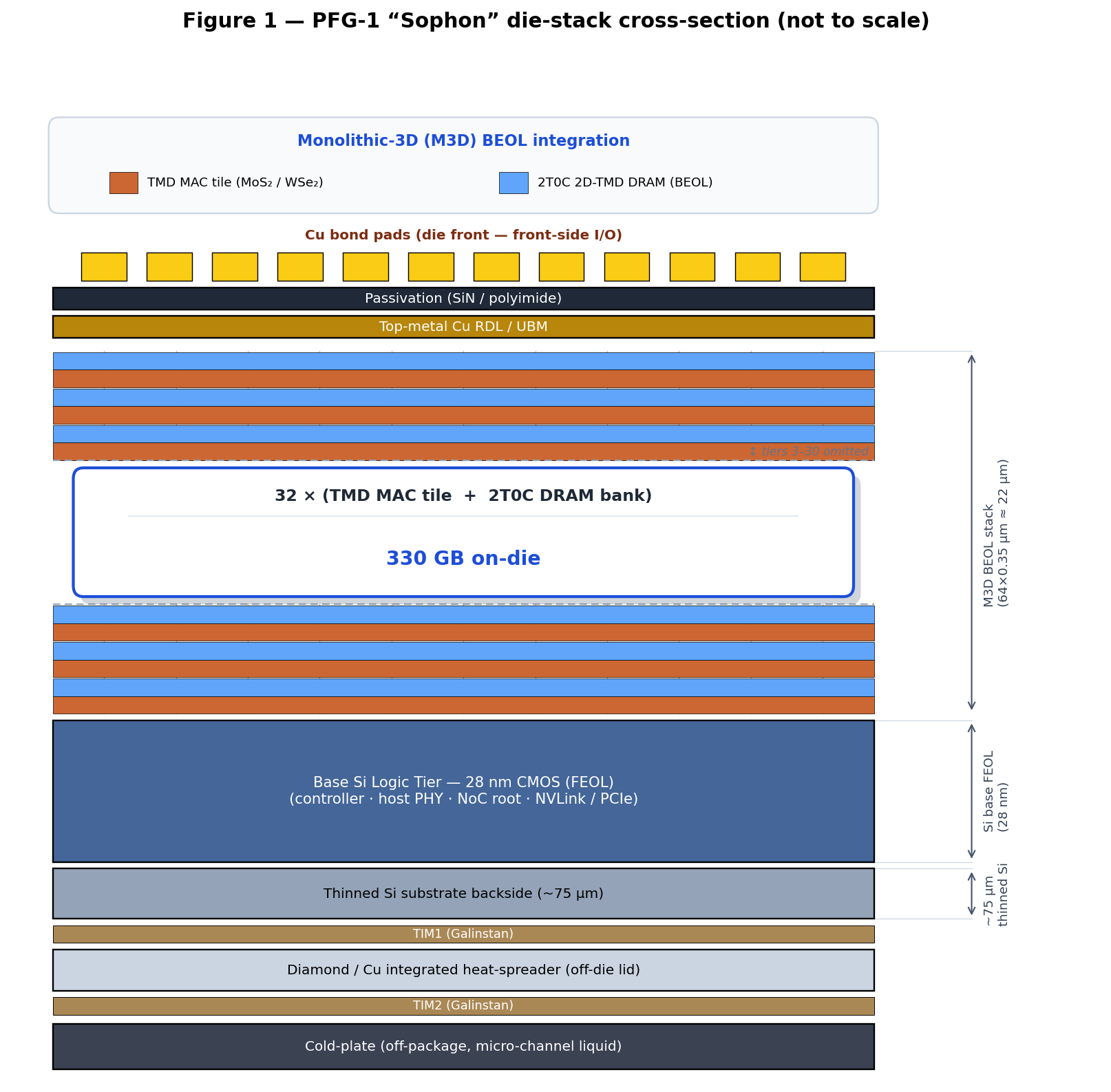
The die can be built on a 28 nm Si Complementary Metal-Oxide-Semiconductor (CMOS) base tier, a 32-tier 2D-TMD CMOS MAC stack, and a Monolithic Inter-tier Via (MIV) fabric [[5]](https://www.phantafield.com/whitepaper#ref-5)[[6]](https://www.phantafield.com/whitepaper#ref-6)[[7]](https://www.phantafield.com/whitepaper#ref-7), with the 2T0C DRAM module embedded at the Back-End-Of-Line (BEOL) Metal-3 layer of each memory tier. The die stack cross-section is shown in **Figure 1**.
!Image 1: Figure 1 — Die stack cross-section
| | **PFG-1 "Sophon"** | | --- | --- | | **Memory** | 2T0C 2D-TMD gain-cell DRAM | | **Compute paradigm** | Pure digital CIM (sense amp + adder tree) | | **Target workload** | Training (fwd + bwd + optimizer) **and** inference (decode + prefill) | | **Capacity** | 330 GB | | **Compute** | 2,100 TFLOPS BF16 (4,200 TFLOPS FP8 inference mode / 8,400 TOPS INT8) | | **Energy / MAC** | **0.620 pJ** (BF16 fwd) / **0.940 pJ** (fwd + bwd) / **0.310 pJ** (FP8 inference) | | **Peak efficiency** | **3.72 TFLOPS/W** (BF16 training avg.) | | **Tokens per watt** | **38.7 tokens/s per W** (80B FP8 decode, 373 W) — ~ 174× an NVIDIA Rubin (R200) or AMD Instinct MI455X at low batch (~ 0.22 tokens/s per W, HBM4-bound) | | **Active power** | ≈ 379 W fwd / ≈ 749 W bwd (~ 564 W training avg.); 373 W FP8 decode | | **80B model perf.** | 2,406 tokens/s training, 0.23 J/tok; 7,219 tokens/s BF16 decode (14,438 tokens/s FP8 mode), 25.8 mJ/tok | | **80B + INT4 + speculative (FP8 mode)** | **72,188 tokens/s effective** | | **BOM** | **$8,358** |
Sophon eliminates off-die High-Bandwidth Memory (HBM) entirely. For 80B-parameter BF16 training it fits weights + first-order optimizer state fully on-die with ~ 10 GB of activation headroom for gradient-checkpointed micro-batches; for inference it serves an 80B model at **7,219 tokens/s** in native BF16 or the full **14,438 tokens/s** in FP8 mode — making it a single train-then-serve part that can be elastically repartitioned between training and serving without changing hardware. Against an NVIDIA Rubin (R200) and an AMD Instinct MI455X — both 2026 HBM4 parts — Sophon delivers **~ 2.7–3.1× higher** 80B batch-1 training throughput per die and **~ 48–53×** higher single-stream FP8 decode throughput, because both GPUs at low batch are HBM-bandwidth-bound at their HBM4 limits (Rubin 22 TB/s, MI455X 19.6 TB/s). Peak dense FLOPS favor the GPUs — Sophon BF16 dense is only ~ 0.21–0.24× their peak — but peak FLOPS do not help at low batch, where weight-memory bandwidth governs.
The architecture delivers **~ 191–214×** the weight bandwidth of an HBM4 package (191× vs Rubin, 214× vs MI455X) — a gap no HBM roadmap closes (Section 7).
The economics follow directly: Morgan Stanley puts a single NVIDIA VR200 (Rubin) NVL72 rack at **≈ $7.8M** — HBM memory alone ≈ $2.0M (25.7% of the rack, +435% over GB300). Sophon eliminates that line item, for a **~ 9.9× / 11.6× lower hardware BOM** than a Rubin / MI455X [[17]](https://www.phantafield.com/whitepaper#ref-17).
- * *
Table of Contents
1. Introduction & Motivation 2. Architecture Overview
- A. Platform (die, tiers, MIV, TMD MAC)
- B. PFG-1 "Sophon" — 2T0C DRAM die
- C. Die floorplan & on-die system organization
- A. Cell geometry & per-tier density
- B. Bandwidth model
- C. Per-MAC energy & power envelope
- D. Digital CIM tile physics & 1/N scaling
4. SPICE Simulation 5. GPU Architecture & AI Performance
- A. Inference
- B. Training
- C. System view
6. Thermal Analysis 7. Scaling Roadmap 8. Energy-Constrained Ceiling on Model Size
- Inference (serving) ceiling
- Training ceiling
9. Economic Analysis 10. Radiation Tolerance for Space Applications 11. Validation, Risks & Future Work 12. References 13. Equations Appendix
- * *
1. Introduction & Motivation
Modern AI accelerators face a memory wall on both workloads they must serve:
**Inference** is _read-dominated_. The model weights are fixed at deployment; every decode step reads the full weight tensor once per generated token. The key metrics are read energy per bit, idle leakage (the model must stay resident between requests), and weight-fetch bandwidth at low batch. Conventional High-Bandwidth Memory (HBM) is bandwidth-bound at low batch: every token's MAC traffic serializes through the ~ 22 TB/s (Rubin) / 19.6 TB/s (MI455X) HBM4 path, and a 288–432 GB HBM4 subsystem draws ~ 10–15 W in self-refresh just to keep the model resident.
**Training** is _read-write symmetric_. Every forward pass reads weights; every backward pass writes gradient updates; the optimizer updates weights in place each step. In-place writability, low write energy, and capacity for both weights _and_ optimizer state are critical. A non-volatile inference-only memory cannot train — for example, Single-Level Cell (SLC) Resistive RAM endurance caps at ~10⁶ cycles, while training an 80B model requires ~10¹⁰ write cycles per parameter.
A **2T0C 2D-TMD gain-cell DRAM** solves both problems with one cell. It exploits the anomalously low off-current density (J off ≈ 10⁻¹⁵ A/µm = 1 fA/µm at 28 nm, i.e. ≈ 0.5 fA per cell) of TMD transistors to obtain **multi-second** retention without an explicit storage capacitor, enabling in-place gradient writes at 20 fJ/bit with **unlimited** write endurance and a refresh overhead of only ≈ 0.08 W. Because the storage node is writable on every cycle, the same die that serves inference can also train; because retention is seconds-long, idle power collapses to ~ 3 W — an inference-grade idle profile on a fully writable training die.
PhantaField's 2D-TMD M3D platform integrates this DRAM module at the BEOL Metal-3 layer of each memory tier, directly above the logic tier whose MAC array consumes its weights.
- * *
2. Architecture Overview
A. Platform
Sophon uses the following physical stack:
| Tier(s) | Function | Process | | --- | --- | --- | | **Base (Si)** | Controller, NoC root, host I/O, PCIe/NVLink PHY | 28 nm bulk Si CMOS |
| **Tiers 1 – 32** | **Interleaved 2D-TMD stack**: 32 logic tiers (MAC array, 750 mm² each) alternating with 32 memory tiers (2T0C DRAM bank, 750 mm² each), forming 32 logic-plus-memory **doublets** | BEOL 2D-TMD (MoS₂ n-FET / WSe₂ p-FET) on odd tiers + DRAM module on even tiers | | **Lid** | Cu / CVD-diamond heat spreader | optional; enables two-side cooling |
Total stack height: **~22 µm** above the Si die (64 tiers × 0.35 µm/tier). The 90 nm-pitch MIV grid provides 1.23 × 10⁸ slots/mm² available inter-tier connections; the design populates only ~5.5 × 10⁵/mm², leaving > 99% MIV headroom.
Tiers are not split within a single layer; instead the 64-tier stack **interleaves dedicated logic and memory tiers** in an A/B/A/B… repeating pattern. Two adjacent tiers form one logic-plus-memory **doublet**; the stack contains 32 such doublets:
- **Logic tiers (32 × 750 mm² = 24,000 mm² total MAC area):** 2D-TMD CMOS MAC array on odd-indexed tiers — MoS₂ n-FETs for NMOS, WSe₂ p-FETs for PMOS. Density 0.175 TFLOPS FP8/mm² (0.0875 TFLOPS BF16/mm²). Clocked at 1.2 GHz, V dd = 0.6 V.
- **Memory tiers (32 × 750 mm² = 24,000 mm² total memory area):** 2T0C 2D-TMD DRAM on even-indexed tiers, fabricated at the Metal-3 BEOL of that tier. Each memory tier sits directly above its paired logic tier; vertical Monolithic Inter-tier Vias (MIVs) on a sub-100 nm pitch carry bit-line/word-line/sense signals straight up from the logic MAC array into the cells, giving every MAC its own private vertical port to local weights with zero NoC traffic. This interleaved arrangement preserves the same total area and capacity as a hypothetical in-tier 50/50 split, while doubling the per-tier MAC routing area and shortening MAC-to-cell signal paths to a single tier-pitch of 0.35 µm.
**Why 2D TMD?** TMD CMOS (MoS₂ / WSe₂) is the only transistor technology that simultaneously offers: (1) BEOL-compatible growth at ≤ 450 °C [[6]](https://www.phantafield.com/whitepaper#ref-6); (2) atomic-scale channel thickness eliminating short-channel leakage [[1]](https://www.phantafield.com/whitepaper#ref-1)[[2]](https://www.phantafield.com/whitepaper#ref-2); (3) electron mobility ≥ 120 cm²/V·s [[4]](https://www.phantafield.com/whitepaper#ref-4); and (4) intrinsic radiation hardness (no buried-oxide trap volume). Critically, the TMD off-current density J off ≈ 10⁻¹⁵ A/µm (1 fA/µm) at 28 nm — i.e. ≈ 0.5 fA for a 0.5 µm-wide cell transistor, roughly 4 orders of magnitude lower than Si NMOS at equivalent gate length [[2]](https://www.phantafield.com/whitepaper#ref-2)[[3]](https://www.phantafield.com/whitepaper#ref-3) — is what enables a 2T0C cell to retain data for **seconds** without any storage capacitor [[8]](https://www.phantafield.com/whitepaper#ref-8)[[9]](https://www.phantafield.com/whitepaper#ref-9), keeping the cell area at 8 F² rather than the ~20 F² needed for a conventional 1T1C DRAM.
B. PFG-1 "Sophon" — 2T0C DRAM die
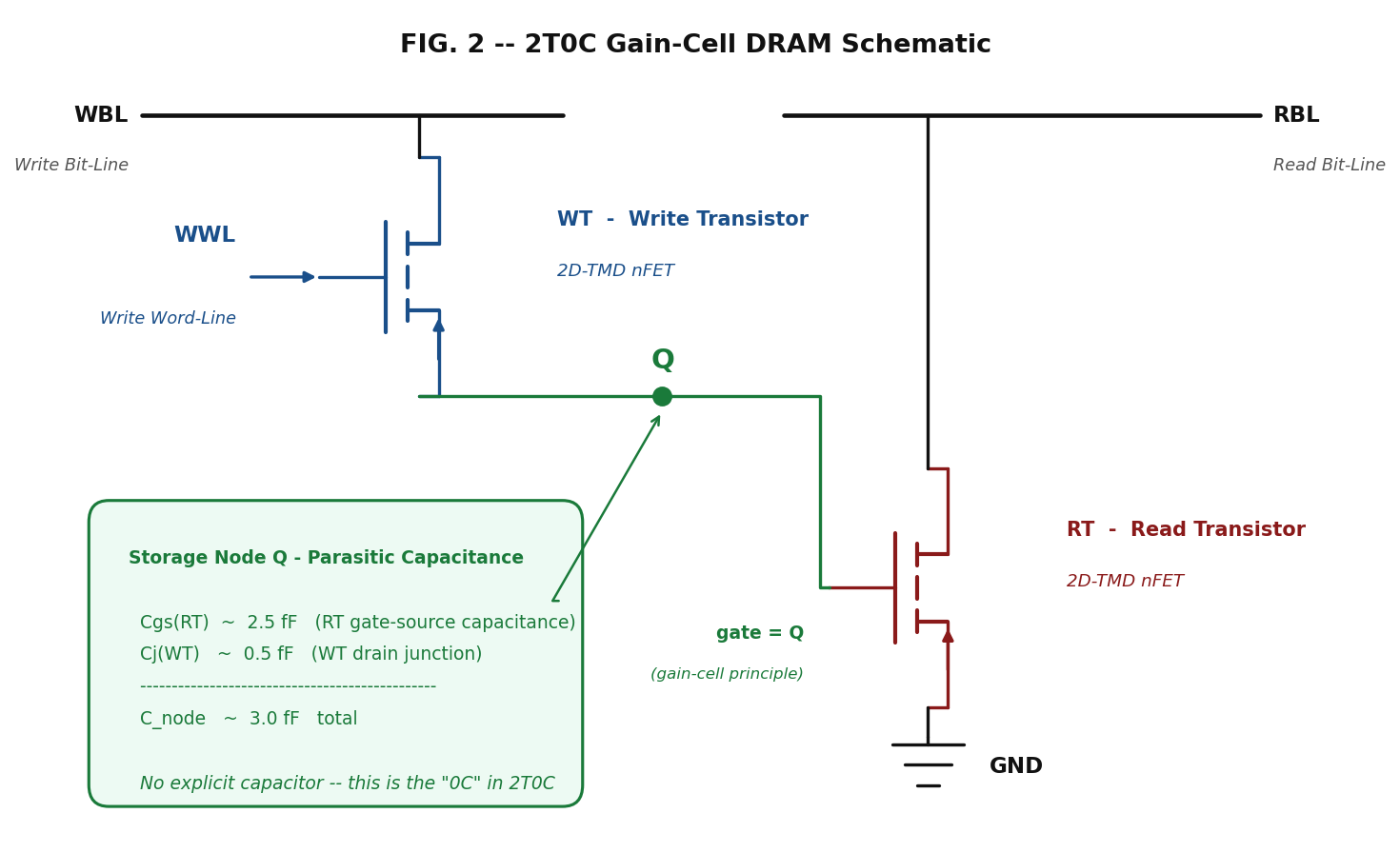
Sophon places a **2T0C 2D-TMD gain-cell DRAM** (8 F², 1 bit/cell) at the Metal-3 BEOL of each memory tier. The cell structure is shown in **Figure 2** and consists of:
!Image 2: Figure 2 — 2T0C gain-cell schematic
- **Write Transistor (WT):** a TMD nFET gated by the Write Word-Line (WWL), which charges the storage node to V dd or discharges it to GND.
- **Read Transistor (RT):** a TMD nFET whose gate is the storage node; its drain current indicates the stored bit.
- **Storage node:** the parasitic gate capacitance of RT (~2.5 fF at 28 nm TMD) plus the junction capacitance of WT's drain (~0.5 fF). No explicit Metal-Insulator-Metal (MIM) or trench capacitor — that is the "0C" in 2T0C.
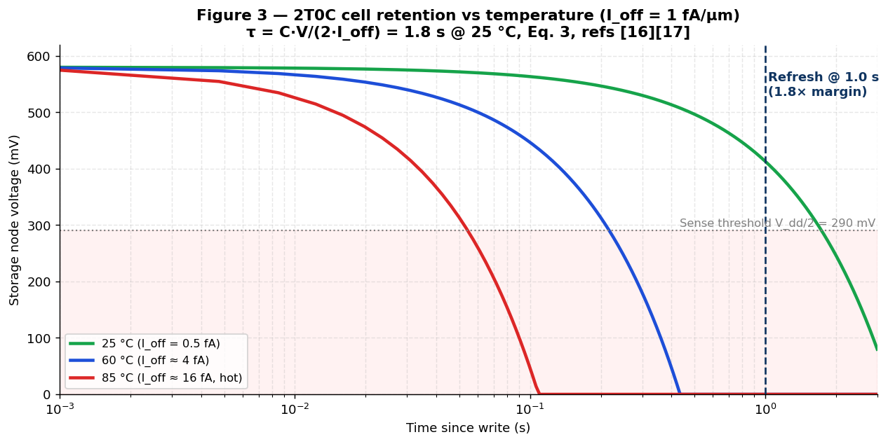
The TMD off-current density of 1 fA/µm (I off ≈ 0.5 fA for a 0.5 µm cell transistor) gives retention τ = C·V dd / (2·I off) = **1.8 s** at 25 °C [[8]](https://www.phantafield.com/whitepaper#ref-8)[[9]](https://www.phantafield.com/whitepaper#ref-9) — see **Eq. 3** and **Figure 3** for the retention curve. Sophon refreshes every **1.0 s** (1.8× margin), consuming only ≈ **0.08 W** for the full 330 GB die (**Eq. 4**). Retention derates ≈ 2× per 10 °C; above 60 °C junction temperature, on-die thermal sensors shorten the refresh interval (≈ 159 ms at 60 °C, ≈ 28 ms at 85 °C), with refresh power staying below ~ 4 W even in the hot corner.
!Image 3: Figure 3 — 2T0C retention vs temperature
Because the storage node is writable on every cycle, Sophon supports in-place BF16 gradient accumulation with unlimited endurance — exactly what training requires — while the same array, read-only, serves the inference decode loop. The die loads a model once and either serves it (inference) or updates it in place (training); a powered-off die reloads its weights from off-die Non-Volatile Memory express (NVMe) at boot (§11.2).
- * *
C. Die Floorplan & On-Die System Organization
The 131,072 CIM tiles are not a flat array — they are partitioned across the 32 logic tiers of the stack (§2.A), exactly **4,096 tiles per logic tier** (derived: 131,072 ÷ 32). Each tile occupies a fixed cell on its tier and is the atomic unit of compute, storage, and redundancy: a 256×256 weight subarray (65,536 weights) feeding a binary sense amp and an 8-level adder tree, with bit-serial activation broadcast at 500 MHz (16 cycles BF16, 8 cycles FP8). The weights for every tile live in the 2T0C cells of the memory tier directly above it (§2.B), so a tile is physically a vertical logic-plus-memory column, not a planar block. A tier is therefore a 4,096-tile mesh of these columns; the full die is 32 such meshes stacked at 0.35 µm pitch, with the 28 nm Si base below carrying everything that is not compute.
**The NoC is a per-tier 2D mesh, not a global fabric.** Each logic tier runs its own mesh router fabric at **≈ 290 TB/s** bisection, and the 64 tiers together present **18,560 TB/s** aggregate (derived: 290 × 64). What rides the NoC is deliberately minimal: **activations and partial sums** — the operands that must move between tiles to assemble a layer's output across the 4,096-tile fan-in. **Weights never touch the NoC.** Every weight is read through its tile's private vertical MIV port — a single tier-pitch hop straight down from the cell to its MAC — delivering 4.2 PB/s of in-tile weight bandwidth with zero shared-bus contention (§2.A). This is the load-bearing asymmetry of the floorplan: the multi-petabyte traffic (weight fetch) is kept entirely vertical and local, so the lateral NoC only ever carries the comparatively small activation/partial-sum flux. The base-tier **NoC root** stitches the per-tier meshes together and bridges them to the controller and host I/O, but it is never in the weight path.
Each tile additionally owns a small **SRAM scratchpad** for activations. Because the NoC carries activations and partials rather than weights, the scratchpad is where a tile stages its inbound activation vector, accumulates its slice of the partial sum across the bit-serial broadcast, and buffers the outbound result before it is handed to the mesh. Holding the live activation working set in fast local SRAM — adjacent to the adder tree, not in the 2T0C DRAM — keeps the broadcast/accumulate inner loop entirely on-tile and lets the 1 Hz-refresh gain-cell DRAM (§2.B) stay dedicated to weights and KV cache, whose access pattern is read-mostly and latency-tolerant by comparison.
**Clock and power are delivered down the 22 µm stack to a low-voltage rail.** The logic tiers are clocked at **1.2 GHz** from a base-tier clock root distributed upward through the MIV grid; the bit-serial activation broadcast runs on a separate 500 MHz domain. Operating at **V dd = 0.6 V** is what makes a 64-tier monolithic stack thermally viable — dynamic power scales with V dd ², so the 0.6 V rail draws ≈ 2.8× less energy than a nominal 1.0 V CMOS rail at the same activity. The trade is current: at fixed power, lowering the voltage raises the supply current, and that current must reach every tier through a power-delivery network (PDN) that climbs the full ~22 µm of stack. Because the design leaves > 99% of the MIV grid unused for signaling (§2.A), those spare vias can be allocated to the PDN (derived) — parallel V dd/GND vias carried straight up to each logic tier hold IR-drop in check across the stack while the bit-serial broadcast switches thousands of tiles in lockstep.
The **28 nm Si base tier** is the system's front door. It carries the controller, the NoC root, host I/O, and the PCIe/NVLink-class PHY — all in mature bulk-Si CMOS, where high-speed analog SerDes and large I/O drivers belong, rather than in the BEOL 2D-TMD tiers above. This separation is what lets the same die both serve and train without hardware change: the host loads a model **once** through the base-tier PHY into the on-die 2T0C DRAM, after which the controller either drives the inference decode loop (weights read-only) or runs in-place gradient writes for training (§2.B) — and a fleet repartitions between the two by command, not by re-spinning silicon. An 80B model — weights, optimizer state, activations, and KV cache — resides entirely on the single die, with every MoE expert resident on-die and only the routed experts drawing power.
| Resource | Per logic tier | Per die (×32 tiers) | | --- | --- | --- | | CIM tiles | 4,096 (derived) | 131,072 | | Weight subarray / tile | 256×256 = 65,536 weights; binary sense amp + 8-level adder tree | | Die footprint | single 750 mm² die — 64 tiers stacked at 0.35 µm (~22 µm tall) | | Logic (MAC) silicon | 750 mm² / tier | 24,000 mm² cumulative (32 × 750, §2.A) | | On-die 2T0C DRAM | 750 mm² / tier | 330 GB total (weights + optimizer + KV cache) | | NoC mesh bisection | ≈ 290 TB/s | 18,560 TB/s aggregate over 64 tiers | | In-tile weight BW (vertical MIV) | 4.2 PB/s — never crosses the NoC | | Activation store | Per-tile SRAM scratchpad (NoC carries activations + partial sums) | | Clock / rail | 1.2 GHz logic, 500 MHz broadcast; V dd = 0.6 V | | Base tier | 28 nm Si — controller, NoC root, host I/O, PCIe/NVLink-class PHY |
- * *
3. Physical Calculations
All formulas are derived in the **Equations Appendix (§13)**. Numeric values reference the equation number in that appendix.
3.A. Cell Geometry & Per-Tier Density
The 64-tier stack **interleaves dedicated logic and memory tiers** in an A/B/A/B… repeating pattern: 32 logic tiers (odd-indexed) and 32 memory tiers (even-indexed), forming 32 logic-plus-memory **doublets**. Each individual tier uses its full 750 mm² footprint for its single role: a logic tier holds the 2D-TMD MAC array (750 mm² MAC); a memory tier holds the co-located 2T0C DRAM bank (750 mm² memory). All capacity and throughput numbers below are reported on a **per-doublet** basis (one logic tier + one memory tier) so they remain directly comparable to the legacy per-tier presentation.
A.1 PFG-1 "Sophon" — 2T0C 2D-TMD gain-cell DRAM weight/gradient cell
The 2T0C gain cell consists of two 2D-TMD transistors and zero explicit storage capacitors [[8]](https://www.phantafield.com/whitepaper#ref-8)[[9]](https://www.phantafield.com/whitepaper#ref-9)[[10]](https://www.phantafield.com/whitepaper#ref-10). It exploits the anomalously low off-current of TMD field-effect transistors — a width-normalized density of **J off = 10⁻¹⁵ A/µm (1 fA/µm)** at 28 nm [[2]](https://www.phantafield.com/whitepaper#ref-2)[[3]](https://www.phantafield.com/whitepaper#ref-3), i.e. only **≈ 0.5 fA** for a 0.5 µm-wide Read Transistor — to retain charge on the gate parasitic of the Read Transistor (RT) for **seconds** without a Metal-Insulator-Metal (MIM) or trench capacitor.
**Cell structure:**
- **Write Transistor (WT):** TMD nFET, gate driven by the Write Word-Line (WWL). Drives the storage node to V dd (write "1") or GND (write "0").
- **Read Transistor (RT):** TMD nFET, gate = storage node, source grounded, drain = Read Bit-Line (RBL). When storage = V dd, RT conducts; when storage = 0, RT is off. Binary current sense.
- **Storage node:** parasitic C gs of RT (~ 2.5 fF) + C junction of WT drain (~ 0.5 fF) = **~ 3.0 fF total**. No explicit capacitor — that is the "0C" in 2T0C.
**Retention physics** (**Eq. 3**, derived from [[8]](https://www.phantafield.com/whitepaper#ref-8)): τ = C node · V dd / (2 · I off). At C node = 3.0 fF, V dd = 0.6 V, and I off = J off · W RT = 1 fA/µm × 0.5 µm = 0.5 fA at 25 °C, τ = **1.8 s**. Sophon refreshes every **1.0 s** (1.8× margin). Retention derates ≈ 2× per 10 °C; above 60 °C junction temperature, on-die thermal sensors shorten the refresh interval (≈ 159 ms at 60 °C, ≈ 28 ms at 85 °C).
| Parameter | Value | Notes | | --- | --- | --- | | Cell footprint | **8 F²** | 2T0C (WT + RT), no capacitor [[10]](https://www.phantafield.com/whitepaper#ref-10) | | Bits per cell | **1 (digital)** | Binary gate state | | Periphery overhead | 45% | Sense amp + refresh controller [[8]](https://www.phantafield.com/whitepaper#ref-8) | | Planar density | **110.0 Mb/mm²** | **Eq. 1**: 1 / (8 × 28² nm² × 1.45) | | Read energy | **30 fJ/bit** | BL precharge + current sense [[28]](https://www.phantafield.com/whitepaper#ref-28) | | Read latency | **3 ns** | Cell access + current sense | | Write energy | **20 fJ/bit** | WT channel charge transfer [[28]](https://www.phantafield.com/whitepaper#ref-28) | | Write endurance | **unlimited** | Gain-cell DRAM — charge-based, no wear-out mechanism [[10]](https://www.phantafield.com/whitepaper#ref-10) | | Retention | **1.8 s @ 25 °C** | Refresh every 1.0 s (**Eq. 3**); I off = 1 fA/µm × 0.5 µm | | Static / refresh power | **≈ 0.08 W** (refresh) | Full 330 GB refreshed at 1 Hz (**Eq. 4**); ~1 W budgeted warm |
**Why a capacitor-less gain cell?** A conventional 1T1C DRAM needs a ~ 20 F² trench/MIM capacitor that is incompatible with low-temperature BEOL M3D integration. The 2T0C cell stores charge on the Read Transistor's own gate parasitic, so it can be built entirely with the same TMD transistors used in the MAC array — no separate capacitor module, no third-party Intellectual Property (IP) license — and the multi-second retention enabled by the 1 fA/µm off-current makes refresh power negligible (≈ 0.08 W, **Eq. 4**).
A.2 Per-doublet and per-die capacity
The stack contains **32 doublets** (one logic tier + one memory tier per doublet). Each doublet contributes one logic-tier's MAC area and one memory-tier's storage area; the total active MAC area and memory area are therefore identical to a hypothetical 64-tier in-tier-split presentation, but routing is denser because each logic tier no longer competes for footprint with its memory bank.
| Item | PFG-1 Sophon (2T0C DRAM) | | --- | --- | | Memory area per memory tier | 750 mm² | | Logic area per logic tier | 750 mm² | | Memory tiers / logic tiers | 32 / 32 | | Capacity per doublet | 10.31 GB | | **Total capacity (32 doublets)** | **330 GB** | | FP8 throughput per logic tier | 131.25 TFLOPS | | BF16 throughput per logic tier | 65.6 TFLOPS | | **FP8 throughput (32 logic tiers)** | **4,200 TFLOPS** | | **BF16 throughput (32 logic tiers)** | **2,100 TFLOPS** | | **INT8 throughput (32 logic tiers)** | **8,400 TOPS** |
Sophon holds 330 GB. For **training**, an 80B-parameter BF16 model (160 GB) plus first-order optimizer state (160 GB for SGD-momentum or Lion) = **320 GB**, leaving **10 GB** for gradient-checkpointed activations (Section 5.B.2). For **inference**, an 80B BF16 model (160 GB) leaves 170 GB free, or an 80B FP8 model (80 GB) leaves 250 GB free for an extended Key-Value (KV) cache or a co-resident draft model (Section 5.A).
A.3 Gain-Cell Read/Write Operation & Sense Margin
Sections A.1 and §2.B describe the _structure_ of the 2T0C cell; this subsection describes how it is _operated_ cycle-by-cycle. The two-transistor topology decouples the write path from the read path entirely — the Write Transistor (WT) owns the storage node, the Read Transistor (RT) only senses it — which is precisely what enables the same array to stream weights to the MAC on every cycle while remaining in-place writable for gradient accumulation (§3.C).
**Write.** A write asserts the Write Word-Line (WWL), turning the WT on and connecting the storage node (RT gate parasitic ~2.5 fF + WT drain junction ~0.5 fF ≈ 3.0 fF) to the Write Bit-Line. The WT channel then charges the node to V dd = 0.6 V for a "1" or discharges it to GND for a "0"; WWL is de-asserted and the TMD off-current (≈ 0.5 fA per 0.5 µm cell) traps that charge for the full retention window. The transferred charge is C node · V dd ≈ 3.0 fF × 0.6 V, and the measured write energy is **20 fJ/bit** — a single channel charge-transfer event, with no high-voltage charge pump and no oxide stress. Because both the value being written and the in-place gradient update (§3.C) take this identical path, training and inference share one write primitive.
**Read — the gain-cell mechanism.** The defining property of the cell is that **RT's gate _is_ the storage node**, so the stored level directly modulates RT's drain conduction. To read, the Read Bit-Line (RBL) is precharged and RT's drain is enabled: a stored V dd turns RT on and sinks current; a stored GND leaves RT off. A **binary sense amplifier** on the RBL resolves the resulting current into a digital bit in ≈ 3 ns at **30 fJ/bit**. Critically, this is a **non-destructive read**: RT senses the node as a _gate voltage_ and draws no charge out of it — unlike a 1T1C cell, where the read dumps the storage capacitor onto the bit-line by charge-sharing and the bit must be written back before the next access. With no write-back cycle, the array can be read back-to-back every cycle, which is exactly how it feeds the 500 MHz bit-serial activation broadcast and the 4.2 PB/s in-tile weight bandwidth (§3.B) without ever stalling for restore.
**Sense margin & why sensing is digital.** The read window is set by RT's on/off drain-current ratio. The same 1 fA/µm TMD off-current that gives multi-second retention also collapses the "0" leg of the read to the sub-femto-amp floor, while the "1" leg conducts at the full TMD on-current — an on/off ratio of many decades. That enormous, deterministic separation means the sense amp only ever has to decide "conducting vs. not," so a single current-comparator threshold suffices: **no ADC, no DAC, no reference ladder**. This is what keeps the read path pure-digital and deterministic end-to-end — there is no analog accumulation to quantize, consistent with the ADC-free CIM tile architecture (§3.D).
**Disturb, retention & endurance during operation.** Because a read is gate-voltage sensing through RT and never discharges the node, **read-disturb is negligible** — a cell can be read arbitrarily many times between refreshes with no charge loss, so the refresh cadence is governed solely by leakage, not by access traffic. Retention τ = C node · V dd / (2 · I off) = **1.8 s** at 25 °C fixes the **1 Hz refresh** (1.8× margin, ≈ 0.08 W for 330 GB; see A.1). Writes are likewise benign: the bit is set by gate-controlled charge transfer through the WT, with **no oxide tunneling and no filament formation**, so there is no wear-out mechanism and endurance is effectively **unlimited** — the enabling condition for streaming in-place gradient writes throughout a full training run (§3.C).
| Property | 2T0C TMD gain cell (Sophon) | Conventional 1T1C DRAM | | --- | --- | --- | | Read type | **Non-destructive** (RT gate-voltage sense) | Destructive (capacitor charge-share onto BL) | | Write-back after read | **None** — read back-to-back every cycle | Required every access (restore) | | Storage element | RT gate parasitic + WT drain junction (≈ 3.0 fF, "0C") | Explicit MIM / trench capacitor | | Sensing | Binary current comparator — no ADC/DAC | Differential charge-sensing amp + reference | | Cell area | **8 F²** | ≈ 20 F² (capacitor-dominated) | | Write endurance | **Unlimited** (gate-controlled charge, no oxide wear) | Unlimited, but every read costs a restore write |
- * *
3.B. Bandwidth Model
Because weights live in memory co-located with their consuming MAC, there is **no global weight-bandwidth pipe**. Sophon employs **fully digital Compute-In-Memory (CIM)** — a sense-amplifier and binary adder tree per column-group. Bandwidth decomposes into orthogonal contributions.
B.1 Weight bandwidth (memory → local MAC)
Each BF16 MAC reads 16 bits from the DRAM bank directly above its tile at 30 fJ/bit with 3 ns latency. The bit-serial multiply runs at the 500 MHz wordline rate over 16 cycles for BF16 (8 cycles in FP8 inference mode); the per-column sense amplifier produces a 1-bit partial product per cycle that feeds an 8-level binary adder tree. A 4-stage pipeline hides DRAM latency.
| Quantity | BF16 (native) | FP8 (inference mode) | | --- | --- | --- | | MAC throughput | 2,100 TFLOPS | 4,200 TFLOPS | | Weight bits per MAC | 16 bits (BF16) | 8 bits (FP8) | | **Aggregate weight BW** | **4.20 PB/s** | **4.20 PB/s** | | Per-tile read width | 275 bits/cycle | 550 bits/cycle | | Memory read latency | 3 ns (4 cycles) | 3 ns (4 cycles) |
Sophon delivers **4.20 PB/s** of aggregate weight bandwidth in either datatype — the byte-rate of weight consumption is the same: 2 bytes/BF16-MAC at 2,100 TFLOPS, or 1 byte/FP8-MAC at 4,200 TFLOPS, both producing 4.20 PB/s. This bandwidth is **in-tile and never crosses the Network-on-Chip (NoC)**.
> **Why is weight bandwidth independent of datatype and of capacity?** In a Compute-In-Memory architecture, weight bandwidth is set by the _MAC array's weight-consumption rate_, which is intrinsic to the **logic tiers**, while capacity is set by the _memory-tier areal density_ (110.0 Mb/mm² for 2T0C DRAM, §3.A). Because every weight is physically co-located with the MAC that consumes it, there is no shared bus whose width would scale with total stored bytes or with bit-depth: a higher-bit datatype simply reads more bits per MAC at a proportionally lower MAC rate. The bandwidth equality is therefore a direct consequence of `BW = (bytes per MAC) × (MAC rate)` being identical for both modes (1 B × 4,200 TFLOPS = 2 B × 2,100 TFLOPS = 4.20 PB/s).
B.2 Gradient bandwidth (training write path)
During the backward pass, accumulated gradients are written back to the DRAM bank at 20 fJ/bit:
| Quantity | Value | | --- | --- | | Gradient write bandwidth | **4.20 PB/s** (mirrors weight read BW) | | Write energy per BF16 gradient | 20 fJ × 16 bits = 320 fJ = **0.32 pJ** | | Backward-pass write power (55% util.) | **370 W** | | Backward-pass write power (100% util.) | **672 W** |
Inference uses the read path only and incurs none of this write power.
B.3 Activation bandwidth (per-tile SRAM scratchpad)
Activations occupy a small per-tile SRAM scratchpad (SPM) (5% of tier area, ~37.5 mm²/tier, ~0.7 GB/tier):
- Per-tier activation bandwidth: ~11,000 GB/s aggregated
- Total activation bandwidth: ~700 TB/s
B.4 NoC bandwidth (inter-tile)
A 2-D mesh NoC routes activations and control. Each tier has its own mesh; vertical MIVs carry inter-layer activations.
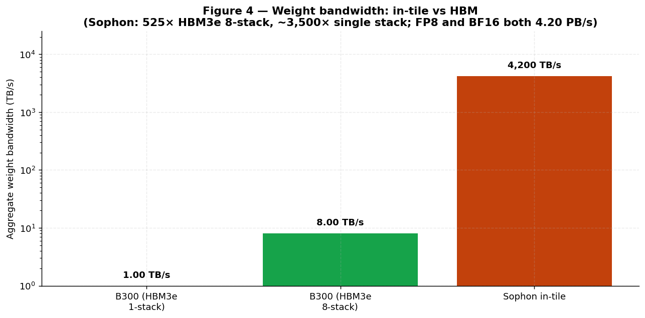
| Path | Bandwidth | | --- | --- | | Per-tier NoC bisection | 290 TB/s | | Aggregate NoC (64 tiers) | 18,560 TB/s | | MIV vertical fabric (weight delivery) | 4,200 TB/s sustained |
B.5 Bandwidth summary
| Path | Sophon | Notes | | --- | --- | --- | | Weight (memory → MAC) | **4.20 PB/s** | In-tile | | Gradient (MAC → memory) | **4.20 PB/s** | In-tile, bwd pass only | | Activation (NoC) | 18,560 TB/s | Inter-tile | | Inter-tier (MIV) | 4,200 TB/s | Vertical (= in-tile weight BW) | | HBM3e reference (8-stack) | 8.0 TB/s | Off-package (NVIDIA Rubin R200) | | HBM4 reference (NVIDIA Rubin R200, 8-stack) | 22 TB/s | Off-package | | HBM4 reference (AMD Instinct MI455X, 8-stack) | 19.6 TB/s | Off-package |
Sophon provides **~ 191× more weight bandwidth** than NVIDIA Rubin (R200) and **~ 214× more** than AMD Instinct MI455X (4,200 TB/s vs 22 TB/s for an 8-stack HBM4 package on Rubin, and 19.6 TB/s for an 8-stack HBM4 package on MI455X [[16]](https://www.phantafield.com/whitepaper#ref-16)[[18]](https://www.phantafield.com/whitepaper#ref-18)) — because that bandwidth is intrinsic to the storage location, not a separate interconnect. **Figure 4** plots the comparison.
3.C. Per-MAC Energy & Power Envelope
C.1 Energy per MAC operation
_Convention note: throughout this paper, "2,100 TFLOPS BF16" and "4,200 TFLOPS FP8" count each multiply-accumulate (MAC) as 2 floating-point operations (one mul + one add) [[16]](https://www.phantafield.com/whitepaper#ref-16). Energies tabulated below are stated **per MAC** (per weight processed), so per-FLOP figures are half the listed values. The chip-power calculations in §C.3 use the per-FLOP convention to align with the TFLOPS rates._
_Architecture note: Sophon uses **pure digital Compute-In-Memory (CIM)**. Each tile contains a per-column sense amplifier feeding an 8-level binary adder tree that produces the partial sum for one row of a 256×256 weight subarray. All multiply-accumulate arithmetic is performed in the binary domain with full deterministic 16-bit (BF16) or 8-bit (FP8) precision — see §3.D for the digital-CIM tile walkthrough and §3.D.2 for why this choice constrains throughput as 1/N in the dense-decode regime._
#### BF16 training MAC
| Component | Energy / MAC | Energy / FLOP | Notes | | --- | --- | --- | --- | | 2T0C DRAM read (16 bits) | **0.480 pJ** | 0.240 pJ | 30 fJ/bit × 16 — BL precharge + binary current sense [[28]](https://www.phantafield.com/whitepaper#ref-28) | | TMD-CMOS digital BF16 MAC | **0.140 pJ** | 0.070 pJ | BF16 adder tree; ~ 2× the per-bit cost of FP8 [[11]](https://www.phantafield.com/whitepaper#ref-11) | | **Total per BF16 forward MAC** | **0.620 pJ** | **0.310 pJ** | forward pass only | | BF16 gradient write (16 bits) | **0.320 pJ** | 0.160 pJ | 20 fJ/bit × 16 — in-place update during backward pass [[28]](https://www.phantafield.com/whitepaper#ref-28) | | **Total per BF16 training MAC** | **0.940 pJ** | **0.470 pJ** | forward + backward combined per weight |
#### FP8 inference MAC
| Component | Energy / MAC | Energy / FLOP | Notes | | --- | --- | --- | --- | | 2T0C DRAM read (8 bits) | **0.240 pJ** | 0.120 pJ | 30 fJ/bit × 8 — half the BF16 read [[28]](https://www.phantafield.com/whitepaper#ref-28) | | TMD-CMOS digital FP8 MAC | **0.070 pJ** | 0.035 pJ | 8-cycle adder tree [[11]](https://www.phantafield.com/whitepaper#ref-11) | | **Total per FP8 inference MAC** | **0.310 pJ** | **0.155 pJ** | forward (read) path only |
The adder-tree compute term is ~ 0.07 pJ/MAC at FP8 — binary additions in modern low-V dd TMD CMOS dissipate roughly 8 fJ per 1-bit add, and an 8-level tree for a 256-input column requires 256 adds amortized across 256 cells (~ 8 fJ/cell × 8 levels = 64 fJ ≈ 0.064 pJ). The pure-digital adder tree avoids the per-sample conversion costs that dominate older mixed-signal CIM designs.
C.2 Static and refresh power
| Source | Sophon | | --- | --- | | Memory static leakage | **0 W** (DRAM has no DC leakage path) | | Memory refresh power | **≈ 0.08 W** (330 GB × 1 Hz × 30 fJ/bit × 8 bits/byte) | | TMD logic leakage | 0 W | | SRAM scratchpad leakage | 1.67 W | | **Total static/idle (model loaded)** | **~ 2 W** |
Sophon's near-zero idle is an operational advantage: an 80B model loaded into Sophon waits for requests at **~ 2–3 W**. An equivalent HBM4-based GPU (e.g. NVIDIA Rubin (R200) with 288 GB, or AMD Instinct MI455X with 432 GB) holds its HBM4 memory subsystem in self-refresh at ~ 10–15 W. With the 2D-TMD off-current at 1 fA/µm (I off ≈ 0.5 fA per cell), the 2T0C retention time rises to 1.8 s and the array needs only a **1 Hz refresh, costing ≈ 0.08 W**. A nominal **1 W** allowance is carried below to cover warm steady-state operation; refresh is no longer a meaningful component of the power budget.
C.3 Active power by phase
#### Inference (read path)
| Phase | DRAM read | Digital MAC array | NoC + SPM | Static | **Chip total** | | --- | --- | --- | --- | --- | --- | | Idle (model loaded) | 0 W | 0 W | 0 W | 2 W | **~ 2 W** | | FP8 decode (55% util.) | 277 W | 81 W | 13 W | 2 W | **≈ 373 W** | | BF16 decode (55% util.) | 277 W | 81 W | 19 W | 2 W | **≈ 379 W** | | FP8 prefill (75% util.) | 378 W | 110 W | 18 W | 2 W | **≈ 508 W** | | Peak FP8 burst (100% util.) | 504 W | 147 W | 28 W | 2 W | **≈ 681 W** |
FP8 decode reads 8-bit weights but runs at twice the BF16 MAC rate (4,200 vs 2,100 TFLOPS), so its read power equals BF16's 277 W (half the bits × double the rate); both are compute-bound at low batch.
#### Training (read + write path)
| Phase | DRAM read | Digital MAC | Refresh | Grad write | NoC + SPM | Static | **Chip total** | | --- | --- | --- | --- | --- | --- | --- | --- | | Idle (model loaded) | 0 W | 0 W | ~1 W | 0 W | 0 W | 2 W | **~ 3 W** | | Forward pass (55% util.) | 277 W | 81 W | ~1 W | 0 W | 18 W | 2 W | **≈ 379 W** | | Backward pass (55% util.) | 277 W | 81 W | ~1 W | 370 W | 18 W | 2 W | **≈ 749 W** | | **Avg. training step (fwd+bwd)** | 277 W | 81 W | ~1 W | 185 W | 18 W | 2 W | **≈ 564 W** | | Peak forward (100% util.) | 504 W | 147 W | ~1 W | 0 W | 36 W | 2 W | **≈ 690 W** | | Peak training (100% fwd+bwd) | 504 W | 147 W | ~1 W | 672 W | 36 W | 2 W | **≈ 1,362 W** |
The training time-average power (forward + backward weighted equally) is **~ 564 W**. With refresh effectively eliminated by the 1 fA/µm off-current, power is dominated by DRAM read + gradient write traffic. Backward pass adds **370 W of gradient write power at 55% utilization** (20 fJ/bit × 16 bits × 2,100 TFLOPS × 55%); idle is **~ 3 W**, giving Sophon an inference-grade idle profile despite being a fully writable training die.
C.4 Efficiency comparison
| Metric | Sophon (inference) | Sophon (training) | NVIDIA Rubin (R200) | AMD Instinct MI455X | | --- | --- | --- | --- | --- | | TFLOPS/W (FP8, peak compute) | 6.2 | — | **~ 9.7** | **~ 11.8** | | TFLOPS/W (BF16, training avg.) | — | 3.72 | **~ 4.86** | **~ 5.88** | | Energy / FP8 inference MAC | **0.310 pJ** | — | ~ 0.21 pJ | ~ 0.17 pJ | | Energy / BF16 forward MAC | — | **0.620 pJ** | ~ 0.41 pJ | ~ 0.34 pJ | | Energy / BF16 training MAC (fwd+bwd) | — | 0.940 pJ | ~ 0.82 pJ | ~ 0.68 pJ | | Energy / decoded token (80B, FP8, B=1) | **25.8 mJ** | — | ~ 4,480 mJ | ~ 4,480 mJ | | Tokens per watt (80B decode, B=1) | **38.7 tokens/s/W** (FP8) | — | ~ 0.22 tokens/s/W | ~ 0.22 tokens/s/W | | Energy / training token (80B, fwd+bwd) | — | **0.23 J** | ~ 40 J (B=1 estimate) | ~ 40 J (B=1 estimate) | | Idle power (80B model loaded) | **~ 3 W** | **~ 3 W** | ~ 10–15 W (memory) | ~ 10–15 W (memory) |
On **peak compute**, the 2026 HBM4 GPUs now lead: Rubin (R200) and MI455X reach ~ 4.86 and ~ 5.88 BF16 TFLOPS/W respectively, roughly 1.3–1.6× Sophon's 3.72 — they pack ~ 4–5× more peak FLOPS behind a 3 nm process. That advantage simply does not help at low batch. For inference, Sophon's FP8-mode decode at 25.8 mJ/token is **~ 174×** lower energy per token than either HBM4 GPU (~ 4,480 mJ/token), because at B=1 both GPUs are HBM-bandwidth-bound and their adder energy is irrelevant — bandwidth, not FLOPS, governs. The digital adder tree keeps per-MAC energy low in both forward and backward passes **and** the 1 fA/µm off-current keeps refresh negligible (≈ 0.08 W), so Sophon spends ~ 3 W at idle vs. ~ 10–15 W for Rubin's 288 GB and MI455X's 432 GB HBM4 subsystems in self-refresh.
3.D. Digital CIM Tile Physics & 1/N Scaling
D.1 Tile geometry
Each Sophon tile is a 256×256 DRAM subarray with co-located digital MAC circuitry. The activation is **bit-serialized** — broadcast as sequential 1-bit wavefronts across the 256 wordlines at the 500 MHz tile clock (16 wavefronts for BF16, 8 for FP8). Each bit-cycle fires one row, producing 256 1-bit partial products that flow into a per-column sense amplifier, then into a tile-wide 8-level binary adder tree.
| Quantity | Value | Notes | | --- | --- | --- | | Subarray geometry | 256 rows × 256 cols | 8 KB of weights per tile (1 bit/cell) | | Tile clock | 500 MHz | Bit-serial activation rate | | Cycles per MAC | 16 (BF16) / 8 (FP8) | One per activation bit | | Per-tile MAC rate | **8 GMAC/s (BF16)** | 256 MACs / 32 ns | | Tiles per die | 131,072 | 2,048 subarrays × 64 tiers | | **Aggregate MAC rate** | **1,050 TMAC/s = 2,100 TFLOPS BF16** | 2,100 TMAC/s = 4,200 TFLOPS FP8 | | Adder tree depth | log₂(256) = 8 levels | ~ 150 ps/level @ 28 nm | | Adder tree latency | **1.2 ns** | Sets the cycle-time floor | | Sense-amp latency | 50 ps | Negligible vs. tree |
In FP8 inference mode the same tile geometry runs an 8-cycle bit-serial activation (vs 16 for BF16), doubling the MAC rate to **4,200 TFLOPS FP8**.
D.2 Why digital CIM still scales as 1/N
A common misconception about CIM is that "all the math happens in parallel inside the memory, so model size shouldn't matter." This is true for **weight transport**, but not for **MAC execution**. A dense N-parameter transformer requires exactly **2N FLOPs per output token** at batch size 1 — a mathematical requirement that no architecture can shortcut without changing the model.
For Sophon FP8 inference at 2,100 TMAC/s aggregate:
| Model size N | MACs / token | Compute time | tokens/s (55% util.) | | --- | --- | --- | --- | | 7 B | 7 GMAC | 6.06 µs | 165,000 | | 70 B | 70 GMAC | 60.6 µs | 16,500 | | 80 B | 80 GMAC | 69.3 µs | **14,438** | | 175 B | 175 GMAC | 152 µs | 6,600 | | 405 B | 405 GMAC | 351 µs | 2,852 |
The slope is **strictly inverse to N** because each weight stored in the DRAM array participates in exactly one MAC per token, and the aggregate MAC ceiling is fixed by the tile count.
D.3 What CIM eliminates vs. what it preserves
| Constraint | NVIDIA Rubin (R200) | AMD Instinct MI455X | Sophon digital CIM | | --- | --- | --- | --- | | Weight transport bandwidth | 22 TB/s HBM4 ceiling | 19.6 TB/s HBM4 ceiling | **none** — in-place | | Weight transport energy | ~ 7 pJ/bit (HBM4 read) | ~ 7 pJ/bit (HBM4 read) | **~ 0.24 pJ/byte** sense (BF16) | | MAC throughput per die | 17,500 TFLOPS FP8 | 20,000 TFLOPS FP8 | **4,200 TFLOPS FP8** | | Energy per FP8 MAC | ~ 1.0 pJ | ~ 1.0 pJ | **0.310 pJ** | | **Compute scaling with N** | **1/N** (bandwidth-bound) | **1/N** (bandwidth-bound) | **1/N** (compute-bound) | | **Energy scaling with N** | **1/N** | **1/N** | **1/N** |
Both fall as 1/N — only the absolute curve height differs. Sophon sits **~ 48× above** NVIDIA Rubin (R200) and **~ 53× above** AMD Instinct MI455X on the FP8-mode decode tokens/s curve because (a) zero weight-transport overhead (Rubin and MI455X decode at low batch are HBM-bandwidth-bound at their 22 TB/s and 19.6 TB/s HBM4 ceilings respectively — only ~ 300 and ~ 270 tok/s for an 80B FP8 model), (b) lower energy per MAC, and (c) sufficient peak MAC throughput at batch-1, where memory bandwidth — not peak FLOPS — governs. Both GPUs in fact carry ~ 4–5× more peak FP8 FLOPS per die than Sophon (Sophon BF16 dense is just 0.24× Rubin and 0.21× MI455X), yet that raw peak buys them nothing at low batch: the weights must still stream over HBM4 every token.
D.4 What WOULD break 1/N — and what we picked
Three architectural or algorithmic paths can break the dense-decode 1/N curve:
1. **Per-cell dedicated MAC units** — give each of the 80 × 10⁹ cells its own dedicated MAC. Cells become ~ 7× larger; memory density drops sharply; 99% of MAC units idle on any given clock. **Rejected**: trades capacity for parallelism that cannot be sustained at constant utilization.
2. **Speculative decoding** — run a small draft model ahead, verify with the large model. Effective speedup of ~ 2.5× when the draft (1 B parameters, ~ 1.25% of Sophon's MAC budget) co-resides on the same die. **Selected as Sophon's default inference deployment mode** — see §5.A.6.
3. **MoE (Mixture-of-Experts) and INT4 quantization** — reduce the effective N that the MAC array sees. MoE shrinks active N by ~ 4–50× (e.g., DeepSeek-V3 671 B → 37 B active ≈ 18×); INT4 halves the cycle count by halving activation bit-depth. **Both supported as first-class workloads**, with combined effective throughput documented in §5.A.6.
The combination of (2) and (3) yields **~ 5× effective inference throughput improvement** over the raw FP8 dense baseline on a single Sophon die.
**Figure 4** plots the weight bandwidth comparison. **Figure 5** decomposes per-MAC energy by component. **Figure 6** shows the resulting active-power breakdown by workload phase.
!Image 4: Figure 4 — Weight bandwidth comparison
!Image 5: Figure 5 — Per-MAC energy decomposition
!Image 6: Figure 6 — Active power breakdown
- * *
D.5 Mapping a Transformer Layer onto the Tile Array
Sections D.1–D.2 fixed the tile geometry and the dense-decode 1/N ceiling; this subsection shows the **dataflow** — how a transformer layer's matmuls physically land on the 131,072 tiles and how partial results are stitched back together. The organizing principle is **weight-stationary execution**: a weight never moves. Every weight matrix _W_ is tiled into 256×256 blocks, and each block is resident in the 2T0C 2D-TMD DRAM doublet sitting _directly above_ its MAC tile. A tile reads its ≈ 64 KB of FP8 weights (256×256 bytes) through a single private vertical MIV hop (§3.A) — there is no NoC traversal, no shared weight bus, and no off-die HBM fetch. This is the source of the 4.2 PB/s in-tile weight bandwidth (§3.C): bandwidth is the product of 131,072 independent ports each one MIV-via deep, not a wide shared channel that must be arbitrated.
Within a tile, computation is **bit-serial** (§D.1). The activation vector is broadcast as sequential 1-bit wavefronts down the 256 wordlines at the 500 MHz tile clock — 8 wavefronts for FP8, 16 for BF16. On each bit-cycle the tile fires one row, the binary sense amps capture 256 1-bit partial products against the stationary weight column, and the 8-level adder tree reduces them to one column partial sum. After the full bit-serial sweep, every tile holds a 256-wide block partial sum for the slice of the output dimension it owns. Because activation is the only thing that flows in and the weight is the only thing that stays, energy per MAC is dominated by the local DRAM read (0.240 pJ of the 0.310 pJ FP8 total, §3.C) rather than by data movement across the die.
A single 256×256 tile covers only a 256-element slab of a real projection, so a full output dimension is assembled by **cross-tile reduction**. Tiles whose blocks share an output row form a reduction group; their partial sums are summed across the on-die NoC (≈290 TB/s per tier, 18,560 TB/s aggregate over 64 tiers, §3.C) and accumulated into the per-tile SRAM activation scratchpad. Only these reduced activations — never weights — travel on the NoC, so the interconnect carries the small O(d model) activation traffic of a layer rather than the O(N) weight traffic that bandwidth-bounds a GPU. The reduced output vector then becomes the broadcast activation for the next layer's tile group, and the layer pipeline advances.
Mapping a complete transformer block follows directly. The four attention projections **W Q/W K/W V/W O** are each laid out as their own contiguous group of weight-stationary tiles; the QK⊤ score and the score·V product run on the same tile fabric with the K and V tensors held in the on-die 2T0C DRAM. Crucially, the **KV cache lives in that same on-die DRAM** as the weights — each decode step writes the new K/V rows in place (20 fJ/bit gradient-class write path, §3.C) and reads the accumulated cache back through the local MIV port, so there is no off-die HBM round-trip per token. The FFN's up/down projections occupy a larger tile group sized to the expansion ratio. For **MoE**, every expert is permanently resident on-die across distinct tile groups (§System): routing does not gather or stream weights — it simply selects _which tiles fire_. Un-routed experts hold their weights stationary and draw only idle power (≈2–3 W), so a sparse 80B-class deployment consumes energy proportional to the active parameter count, not the resident parameter count — the mechanism behind the MoE energy-ceiling analysis and the serving curves of (§5.A).
The same physical tiles run **train-then-serve** with no hardware change. In serving mode the DRAM is read-only: activations sweep forward through the projection and FFN/MoE groups, the KV cache grows in place, and decode draws ≈373 W (FP8). In training mode the identical tiles run the forward pass and then the backward pass over the writable 2T0C DRAM, performing **in-place gradient accumulation** through the dedicated grad-write path (0.320 pJ of the 0.940 pJ BF16 training MAC, §3.C) — weights are updated where they sit, again with no weight transport. Because the only difference between the two modes is whether the local DRAM port is exercised read-only or read-modify-write, a fleet repartitions between training and serving purely in software: a die that trained a checkpoint at midnight can serve it at noon on exactly the same tile array (§5.A).
- * *
4. SPICE Simulation
All circuits simulated in **ngspice 41** at 25 °C, Level-1 MOSFET models tuned to published 2D-TMD measurements [[1]](https://www.phantafield.com/whitepaper#ref-1)[[2]](https://www.phantafield.com/whitepaper#ref-2)[[3]](https://www.phantafield.com/whitepaper#ref-3).
4.1 2T0C gain-cell DRAM
Setup: write `1` at t = 0; hold; read at t = 1.0 s.
| Metric | Result | | --- | --- | | Storage-node voltage after write | 0.58 V (V t-drop limited; RT threshold ~0.4 V) | | Storage-node voltage at t = 1.0 s | **433 mV** (133 mV margin above V dd/2 sense threshold) | | Retention (closed-form, I off = 0.5 fA @ 1 fA/µm × 0.5 µm) | **1.8 s** | | Sense energy | **30 fJ/bit** | | Write energy (WT charging node) | **20 fJ/bit** |
The stored voltage at the 1.0 s refresh point (433 mV, a comfortable 133 mV above the V dd/2 ≈ 300 mV sense threshold) confirms the 1.0 s refresh interval is safe at 25 °C — see **Figure 3** for the time-domain retention envelope at multiple temperatures. Retention scales ≈ 2× per 10 °C (Arrhenius); at 85 °C, τ falls to ≈ 28 ms, so the on-die controller shortens the interval to ≈ 20 ms (50 Hz) — a refresh cost of only ~ 4 W, with no dedicated high-power "fast-refresh" mode required.
4.2 Latch sense-amplifier
Binary current sense: a single latch fired against a fixed mid-point reference. The 1-bit output drives directly into the per-tile binary adder tree.
| Metric | Result | | --- | --- | | Resolve time (50 mV differential → rail) | **15 ps** | | Differential gain | ≥ 150 | | Read energy per bit | **30 fJ** | | Read latency (cell + sense) | **3 ns** |
4.3 Thermal RC
34-node thermal network solved at DC for peak training power injection (749 W backward pass). Stack ΔT remains sub-Kelvin; package resistance dominates (see Section 6).
- * *
5. GPU Architecture & AI Performance
The head-to-head comparison against the two 2026 HBM4 flagships — NVIDIA Rubin (R200) and AMD Instinct MI455X [[16]](https://www.phantafield.com/whitepaper#ref-16)[[17]](https://www.phantafield.com/whitepaper#ref-17) is summarized in **Figure 7**.
!Image 7: Figure 7 — PFG-1 vs Rubin (R200) / MI455X
5.1 Die stack overview
| Layer | Function | Process | Notes | | --- | --- | --- | --- | | Base Si | Controller, NVLink PHY, PCIe, NoC root | 28 nm CMOS | 100 µm thick | | Tiers 1–64 | **Interleaved**: 32 logic tiers (2D-TMD MAC array) + 32 memory tiers (2T0C DRAM), alternating A/B/A/B… | 2D-TMD M3D | 0.35 µm/tier; 32 doublets |
- * *
5.A. Inference
Sophon serves inference on the same silicon it trains on. The MAC array supports both native BF16 (the training datatype) and an FP8 inference mode (4,200 TFLOPS / 8,400 INT8 TOPS); FP8 is the recommended serving mode because it doubles decode throughput, halves energy/token, and frees capacity. The model loads once and serves indefinitely; a powered-off die reloads from NVMe at boot (§11.2).
#### 5.A.1 Architecture summary
| Parameter | Value | | --- | --- | | Memory | 330 GB 2T0C DRAM (on-die) | | On-die capacity | **330 GB** | | FP8 throughput | **4,200 TFLOPS** | | INT8 throughput | **8,400 TOPS** | | BF16 throughput | **2,100 TFLOPS** | | Energy / FP8 MAC | **0.310 pJ** | | Idle power | **~ 3 W** |
#### 5.A.2 80B model fit
- 80B params × FP8 (1 byte/param) = **80 GB** — fits in 330 GB with **250 GB headroom**.
- 80B params × BF16 (2 bytes/param) = **160 GB** — fits in 330 GB with **170 GB headroom**.
- Headroom available as: static extended Key-Value (KV) cache, a co-resident speculative draft model, or long-context prefill buffer.
- A 320B-parameter INT4 model = ~ 160 GB — also fits on a single Sophon die.
#### 5.A.3 Decode performance
Decode is compute-bound from batch size B = 1 because weights reside in-tile — no off-die memory traffic at any batch size. **The "Aggregate tokens/s" column is the total tokens emitted per second by the die across all batch slots; per-replica throughput is aggregate / B.** Figures below are for FP8 inference mode (the recommended serving point); BF16 native serving is exactly half.
| Batch (B) | Aggregate tokens/s (FP8) | Per-replica tokens/s | Notes | | --- | --- | --- | --- | | 1 | **14,438** | 14,438 | 4,200 TFLOPS × 55% / (2 × 80B FLOP/tok) | | 8 | **14,438** | 1,805 | compute-bound; aggregate unchanged | | 32 | **14,438** | 451 | | | 128 | **14,438** | 113 | |
In native **BF16** the same 80B model decodes at **7,219 tokens/s** (B = 1) — exactly half the FP8 rate because BF16 doubles the bit-serial cycle count (16 vs 8). Because every batch slot reads from the same in-tile DRAM, batching does not increase aggregate throughput; it amortizes prefill cost across multiple requests.
#### 5.A.4 Power and energy
| Phase | Chip power | Energy / token | | --- | --- | --- | | Idle (model loaded) | **~ 3 W** | — | | FP8 decode (B = 1, 55% util.) | **≈ 373 W** | **25.8 mJ** | | BF16 decode (B = 1, 55% util.) | **≈ 379 W** | **52.5 mJ** | | FP8 prefill (75% util.) | **≈ 508 W** | — | | FP8 peak burst (100% util.) | **≈ 681 W** | — |
Sustained FP8 prefill: **~ 19,690 tokens/s** (75% utilization); a 2,000-token prompt completes in ~ 102 ms.
#### 5.A.5 Comparison with NVIDIA Rubin (R200) and AMD Instinct MI455X
| Metric | NVIDIA Rubin (R200) | AMD Instinct MI455X | **Sophon (FP8)** | **Sophon (BF16)** | Ratio (FP8) vs Rubin / MI455X | | --- | --- | --- | --- | --- | --- | | Process | TSMC N3 (HBM4) | TSMC N3 (HBM4) | 28 nm + 2D-TMD M3D | 28 nm + 2D-TMD M3D | — | | Memory | 288 GB HBM4 | 432 GB HBM4 | **330 GB 2T0C DRAM** | **330 GB 2T0C DRAM** | **1.15×